Lithographic apparatus and method

A technology of lithography equipment and heaters, which can be used in microlithography exposure equipment, optomechanical equipment, optics, etc., and can solve problems such as thermal expansion.

Active Publication Date: 2011-09-21
ASML NETHERLANDS BV
View PDF17 Cites 19 Cited by
  • Summary
  • Abstract
  • Description
  • Claims
  • Application Information

AI Technical Summary

Problems solved by technology

These thermal loads may cause ...

Method used


Image

  • Lithographic apparatus and method
  • Lithographic apparatus and method
  • Lithographic apparatus and method

Examples


Embodiment Construction

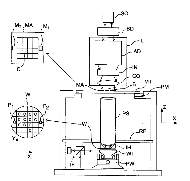
[0049] figure 1 A lithographic apparatus according to an embodiment of the invention is schematically shown. The lithography equipment includes:

[0050] - an illumination system (illuminator) IL configured to condition a radiation beam B (eg, ultraviolet (UV) radiation or deep ultraviolet (DUV) radiation);

[0051] - a support structure (e.g. a mask table) MT configured to support a patterning device (e.g. a mask) MA and connected to first positioning means PM configured to precisely position the patterning device according to determined parameters;

[0052] - a substrate table (e.g. a wafer table) WT configured to hold a substrate (e.g. a resist-coated wafer) W and associated with a second positioning device configured to precisely position the substrate according to determined parameters PW connected; and

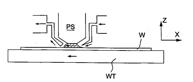
[0053] - A projection system (eg a refractive projection lens system) PS configured to project the pattern imparted to the radiation beam B by the patterning device ...


PUM


Abstract

The invention discloses a lithographic apparatus and method. The lithographic apparatus includes a substrate table configured to support a substrate on a substrate supporting area and a heater and/or temperature sensor on a surface adjacent the substrate supporting area.

Description

technical field [0001] The invention relates to a lithographic apparatus and a method of compensating for local thermal load variations. Background technique [0002] A lithographic apparatus is a machine that applies a desired pattern to a substrate, usually a target portion of the substrate. For example, lithographic equipment may be used in the manufacture of integrated circuits (ICs). In this case, a patterning device, alternatively referred to as a mask or reticle, may be used to generate the circuit pattern to be formed on the individual layers of the IC. The pattern can be transferred onto a target portion (eg, comprising a portion, one or more dies) on a substrate (eg, a silicon wafer). Typically, the pattern is transferred by imaging the pattern onto a layer of radiation sensitive material (resist) provided on the substrate. Typically, a single substrate will contain a network of adjacent target portions that are successively patterned. Known lithographic appara...

Claims


Application Information

Patent Timeline
IPC IPC(8): G03F7/20
CPCG03F7/70875G03F7/202G03F7/7085H01L21/0274
Inventor N·坦凯特J·J·奥腾斯B·A·W·H·柯拿伦R·J·伍德G·F·尼诺M·J·里米J·H·W·雅各布斯T·S·M·劳伦特J·G·C·昆尼
Owner ASML NETHERLANDS BV
Why Eureka
Try Eureka