

Gallium nitride based light-emitting diode (LED) epitaxial wafer and growth method thereof
An LED epitaxial wafer, GaN-based technology, applied in electrical components, circuits, semiconductor devices, etc., can solve the problems of dielectric melting, deterioration of LED performance parameters, leakage and other problems
- Summary
- Abstract
- Description
- Claims
- Application Information
AI Technical Summary
Problems solved by technology
Method used
Image

Examples
Embodiment 1
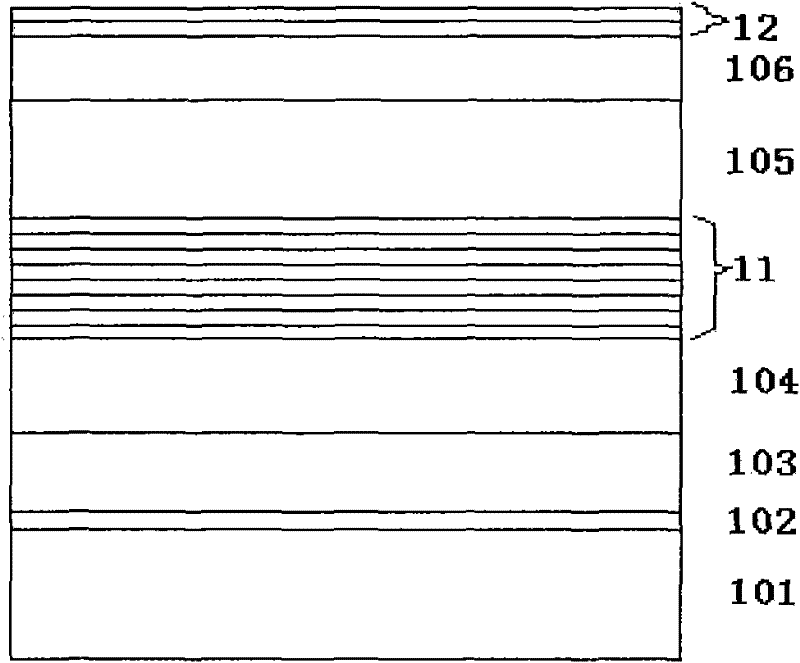
[0025] 1. Put the sapphire substrate with (0001) crystal orientation into the reaction chamber, and then 2 The temperature in the environment is raised to 1050° C., stabilized for 10 minutes, and the substrate is purified at high temperature.
[0026] 2. Lower the temperature to 530° C. to grow a low-temperature GaN-based buffer layer with a thickness of 20 nm.
[0027]3. Raise the temperature to 1100°C to grow non-doped gallium nitride with a thickness of 1 μm.
[0028] 4. Grow n-type gallium nitride with a thickness of 1.5 μm at 1100° C.
[0029] 5. In N 2 The multi-quantum well layer is grown for 10 periods in the environment, the GaN barrier layer: the thickness is 20nm, the growth temperature is 850°C; the InGaN well layer: the thickness is 2nm, the growth temperature is 810°C.
[0030] 6. Raise the temperature to 960°C to grow p-type Al with a thickness of 30nm 0.15 Ga 0.85 N layers.
[0031] 7. Grow p-type gallium nitride with a thickness of 150 nm at 940°C.
[0...
Embodiment 2
[0036] Growth by MOCVD method: except step 8, other steps are as shown in Example 1. And step 8 is:
[0037] 8. Grow low-doped n-type In with a thickness of 2nm at 810°C 0.1 Ga 0.9 N and 2nm highly doped n-type In 0.2 Ga 0.8 N-electrode contact layer.
[0038] In this embodiment, the 300×300 μm chip made by the standard chip process 2 The chip with ITO as the transparent electrode has a reverse 4000V ESD yield of 90%.
Embodiment 3
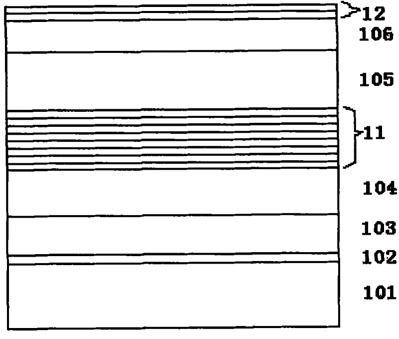
[0040] Grown by MOCVD method.
[0041] 1. Put the sapphire substrate with (0001) crystal orientation into the reaction chamber, and then 2 The temperature in the environment is raised to 1050° C., stabilized for 10 minutes, and the substrate is purified at high temperature.
[0042] 2. Lower the temperature to 530° C. to grow a low-temperature GaN-based buffer layer with a thickness of 20 nm.
[0043] 3. Raise the temperature to 1100°C to grow non-doped gallium nitride with a thickness of 1.5 μm.
[0044] 4. Grow n-type gallium nitride with a thickness of 2 μm at 1100°C.
[0045] 5. In N 2 The multi-quantum well layer is grown for 5 periods in the environment, the GaN barrier layer: the thickness is 20nm, the growth temperature is 850°C; the InGaN well layer: the thickness is 1.6nm, the growth temperature is 810°C.
[0046] 6. Raise the temperature to 960°C to grow p-type Al with a thickness of 30nm 0.15 Ga 0.85 N layers.
[0047] 7. Grow p-type gallium nitride with a t...
PUM
| Property | Measurement | Unit |
|---|---|---|
| Thickness | aaaaa | aaaaa |
| Thickness | aaaaa | aaaaa |
| Thickness | aaaaa | aaaaa |
Abstract
Description
Claims
Application Information