Producing method of overlay ceramic electronic component

A manufacturing method and technology of electronic components, applied in fixed capacitor parts, laminated capacitors, fixed capacitor electrodes, etc., can solve problems such as poor short circuit, erosion, and reduced coverage of internal electrodes, and achieve high reliability and coverage High, no bad effect of short circuit

Inactive Publication Date: 2011-09-28
MURATA MFG CO LTD
View PDF4 Cites 5 Cited by
  • Summary
  • Abstract
  • Description
  • Claims
  • Application Information

AI Technical Summary

Problems solved by technology

[0004] In the case of this method, the cured ceramic green sheet (for example, the first-layer ceramic green sheet) can be hardly attacked by the solvent contained in the ceramic green sheet (for example, the second-layer ceramic green sheet) formed thereon ( attack), but the internal electrode pattern formed on the first layer of ceramic green sheet is eroded by the solvent in the ceramic slurry for forming ceramic green sheet coated later, and the coverage of th

Method used


Image

  • Producing method of overlay ceramic electronic component
  • Producing method of overlay ceramic electronic component
  • Producing method of overlay ceramic electronic component

Examples


Embodiment 1

[0061] [1] Production of multilayer ceramic capacitors (sample No. 1 in Table 1) according to Examples of the present invention

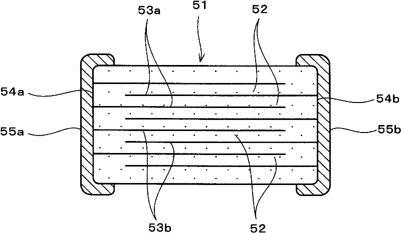
[0062] In this Example 1, a typical laminated ceramic electronic part having figure 1 The case of a multilayer ceramic capacitor having the structure shown will be described as an example.

[0063] Such as figure 1 As shown, this multilayer ceramic capacitor has a structure in which, in a multilayer ceramic element (capacitor element) 51, a plurality of internal electrodes 53a, 53b are stacked with a ceramic layer 52 interposed therebetween, and the internal electrodes 53a, 53b facing each other with the ceramic layer 52 interposed therebetween 53b is drawn out alternately to end surfaces 54a, 54b on different sides of multilayer ceramic element 51, and is connected to external electrodes 55a, 55b formed on the end surfaces.

[0064] (1-1) Production of internal electrode paste

[0065] As a conductive component constituting the internal electrod...

Embodiment 2

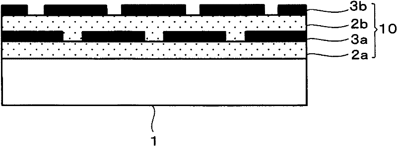
[0145] In this second example, the first internal electrode pattern is formed on the substrate (support film), and the first dielectric green sheet (ceramic green sheet), the second internal electrode pattern, and the second dielectric green sheet are sequentially stacked thereon. sheets (ceramic green sheets) to form a multilayer structural unit, and a multilayer ceramic capacitor is produced by laminating a predetermined number of the multilayer structural units. In addition, in the case of this Example 2, similarly to the case of the above-mentioned Example 1, a figure 1 Multilayer ceramic capacitors of the configuration shown. It will be explained below.

[0146] In this Example 2,

[0147] As (a) a ceramic slurry for forming a dielectric green sheet, and

[0148] (b) an internal electrode paste for forming an internal electrode pattern,

[0149] The same materials as those used in Example 1 above were used.

[0150] First, if Figure 4 As shown, the internal electro...

Embodiment 3

[0164] In this Example 3, as Image 6 As shown in FIG. The dielectric paste for the stepped absorption layer was dried at 60° C. for 5 minutes to form the dielectric pattern for the stepped absorption layer (stepped absorption layer) 20 , and a multilayer ceramic capacitor was produced in the same manner as the multilayer ceramic capacitor of Example 1.

[0165] In addition, in Image 6 , labeled with figure 2 Parts with the same symbols represent the same or corresponding parts.

[0166] For the multilayer ceramic capacitor of Example 3, the coverage of internal electrodes, electrical characteristic defect rate (short circuit defect rate), and structural defect occurrence rate were inspected by the same method as in the case of Example 1 above. As a result, similar to the case of the sample No. 1 in Table 1 of Example 1 (the sample related to the example of the present invention), it was confirmed that a high coverage of the internal electrodes and a high electrical chara...


PUM

PropertyMeasurementUnit
Thicknessaaaaaaaaaa
Particle sizeaaaaaaaaaa

Abstract

The invention provides a producing method of an overlay ceramic electronic component, which can prevent internal electrode patterns from erosion by solvents in ceramic slurry when ceramic raw slices are formed by coating ceramic slurry, is free of problems like reduced coverage rate and short circuit of internal electrodes, and can really manufacture overlay ceramic electronic components with high reliability. Each time when internal electrode patterns (3a, 3b) contacting with the ceramic slurry are formed, internal electrode slurry having solidifying resin and conductive components is adopted according to a manner enabling the slurry to become regulated patterns, and the solidifying resin is solidified.

Description

technical field [0001] The present invention relates to a method of manufacturing a laminated ceramic electronic component manufactured through the steps of forming a ceramic green sheet by applying a ceramic slurry and applying an internal electrode paste in a predetermined pattern. Internal electrode patterns are formed. Background technique [0002] As one of the methods of manufacturing laminated ceramic electronic components having a structure in which ceramic layers and internal electrode layers are alternately laminated such as laminated ceramic capacitors, it has been proposed to laminate lower green sheets (lower ceramic green sheets) and form A method of manufacturing a laminated electronic component by forming a green chip (green chip) by forming a laminate unit including an internal electrode pattern layer on it, and firing the green chip (Patent Document 1). [0003] Furthermore, Patent Document 1 discloses that after curing the lower green sheet containing a c...

Claims


Application Information

Patent Timeline
IPC IPC(8): H01G4/30H01G4/008H01G4/12
Inventor 户上敬藤冈真人吉川宣弘
Owner MURATA MFG CO LTD
Why Eureka
Try Eureka