STI (Shallow Trench Isolation) structure and manufacturing method thereof

A trench isolation and trench technology, applied in electrical components, semiconductor/solid-state device manufacturing, circuits, etc., can solve the problems of reduced trench isolation function, short circuit of semiconductor devices, high sensitivity of trench 20 shape, and achieve isolation performance Good, enlarged aspect ratio effect

Inactive Publication Date: 2011-09-28
SEMICON MFG INT (SHANGHAI) CORP
View PDF2 Cites 8 Cited by
  • Summary
  • Abstract
  • Description
  • Claims
  • Application Information

AI Technical Summary

Problems solved by technology

[0007] However, if figure 2 As shown, the problem existing in the existing subatmospheric pressure chemical vapor deposition method is that the conformal growth characteristic of the subatmospheric pressure chemical vapor deposition film is mainly to fill the trench 20 by growing from the sidewall 22 of the trench 20 to the middle, so The sensitivity to the profile of the etched trench 20 is very high. If the etched trench 20 is recessed into the sidewall 22, a band will eventually be formed in the tight seam (seam) 50 formed in the middle of the trench 20 of the semiconductor substrate 10. The gap 51 of the hole, and the defect of the gap 51 cannot be removed by annealing, and is easily corroded by the solution in the subsequent cleaning step, resulting in the connection of the trench, reducing the isolation function of the trench, and causing a short circuit between subsequent semiconductor devices

Method used


Image

  • STI (Shallow Trench Isolation) structure and manufacturing method thereof
  • STI (Shallow Trench Isolation) structure and manufacturing method thereof
  • STI (Shallow Trench Isolation) structure and manufacturing method thereof

Examples


Embodiment Construction

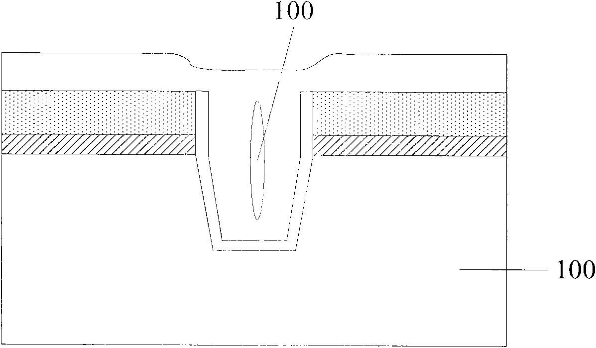
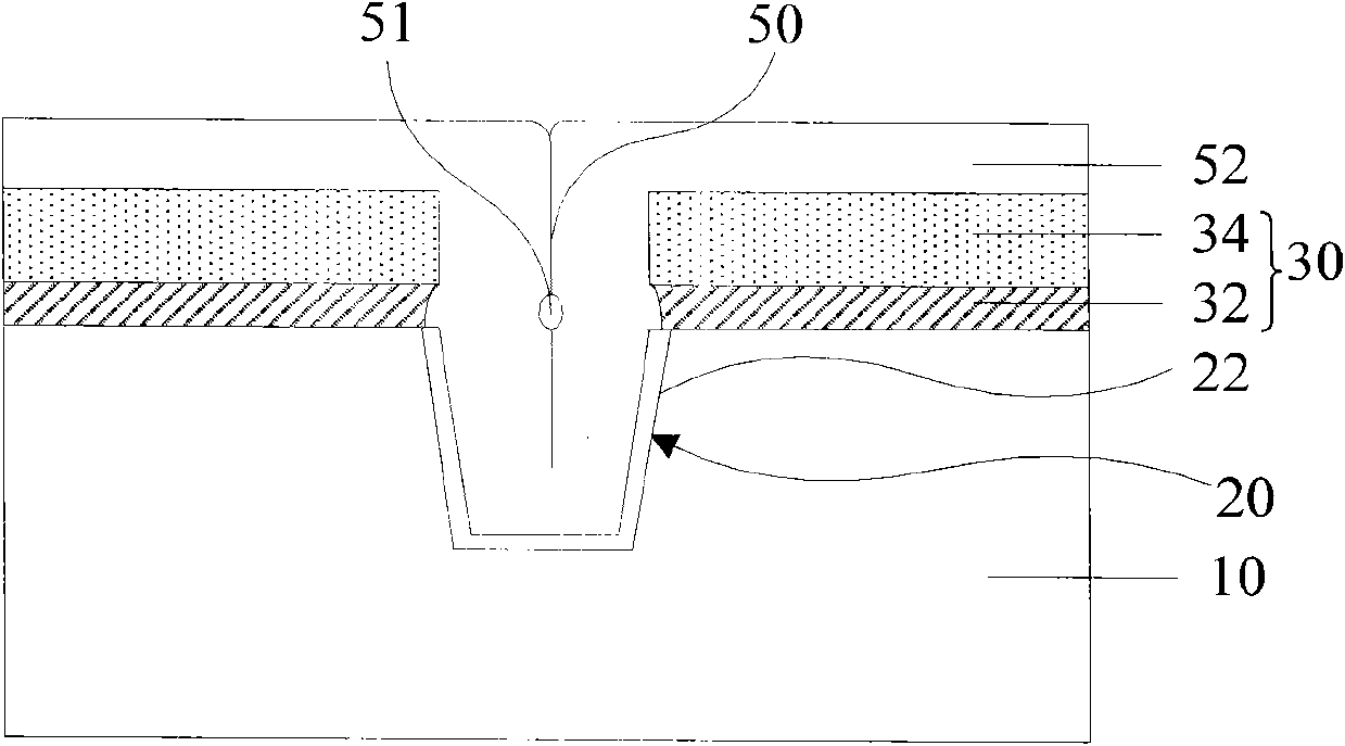
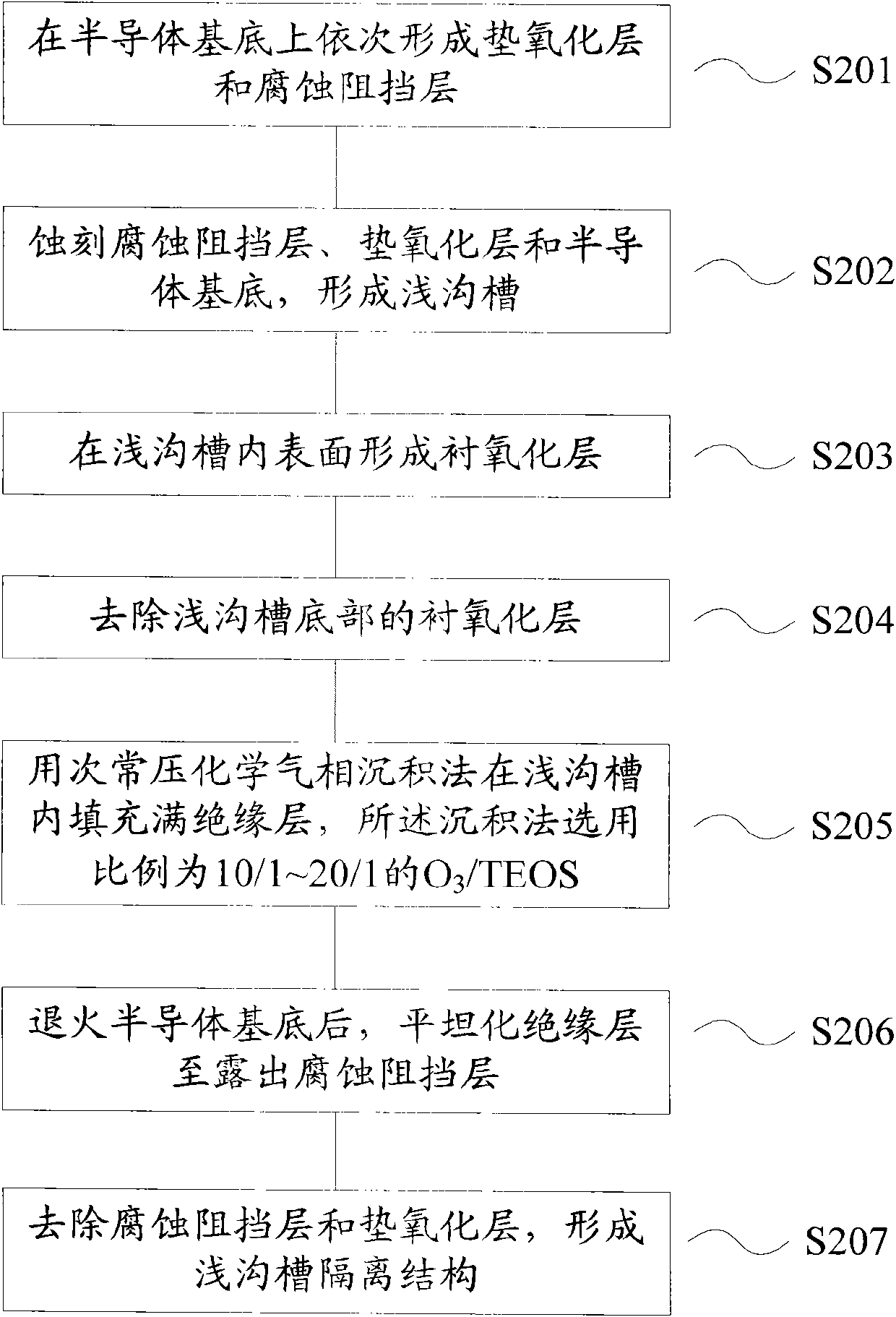
[0024] The core of the present invention is to first deposit the first insulating layer to fill the trenches by sub-atmospheric pressure chemical vapor deposition, and then remove part of the first insulating layer that is prone to gap defects, and then use wet etching to remove part of the liner nitride layer Make it the same depth as the first insulating layer, and finally deposit the second insulating layer to fill the trench. Using the method, the complete filling of the bottom of the trench with high aspect ratio is realized, and during the process of depositing the second insulating layer, Since the depth of the trench is reduced and the width is increased (part of the liner nitride layer is removed from the sidewall of the trench), filling of the trench is easier to implement and avoids the defects of possible gaps in the prior art.

[0025] The specific embodiments of the present invention will be described in detail below in conjunction with the accompanying drawings. ...


PUM

PropertyMeasurementUnit
thicknessaaaaaaaaaa

Abstract

The invention discloses a manufacturing method of an STI (Shallow Trench Isolation) structure. The manufacturing method comprises the following steps of: forming a hard mask layer on a semiconductor substrate; etching the hard mask layer and the semiconductor substrate to form a shallow trench; forming an oxide lining layer on the sidewall of the shallow trench and forming nitride lining layers on the oxide lining layer and the hard mask layer; depositing a first insulating layer, filling of the shallow trench and covering the oxide lining layer; carrying out an annealing process and flattening the first insulating layer to expose the nitride layer; removing a part of the first insulating layer in the shallow trench by carrying out a first wet etching process; removing the nitride lining layer on the hard mask layer by carrying out a second wet etching process to enable the height of the nitride lining layer on the sidewall of the shallow trench to be equal to the height of the first insulating layer; depositing a second insulating layer, filling of the shallow trench and covering the hard mask layer; and removing the second insulating layer and the hard mask layer on the semiconductor substrate to form the STI structure. Through the manufacturing method disclosed by the invention, the generation of seams in the shallow trench can be avoided.

Description

technical field [0001] The invention relates to a manufacturing method of a semiconductor device, in particular to forming a trench isolation structure and a forming method thereof. Background technique [0002] As the size of integrated circuits decreases, the devices that make up the circuits must be placed more densely to fit the limited space available on the chip. As current research focuses on increasing the density of active devices per unit area of ​​a semiconductor substrate, effective insulation between circuits becomes more important. Currently, commonly used methods for forming isolation regions mainly include a local oxidation isolation (LOCOS) process and a shallow trench isolation (shallow trench isolation, STI) process. [0003] Compared with the local oxidation isolation (LOCOS) process, the trench isolation technology has a number of electrical isolation advantages, including reducing the area occupied by the silicon wafer surface while increasing the inte...

Claims


Application Information

Patent Timeline
Patent Type & Authority Applications(China)
IPC IPC(8): H01L21/762
Inventor 郑春生
Owner SEMICON MFG INT (SHANGHAI) CORP
Why Eureka
Try Eureka