Low-heat-resistance packaging structure of power MOS (Metal Oxide Semiconductor) device

A technology of MOS device and packaging structure, which is applied to electric solid-state devices, semiconductor devices, semiconductor/solid-state device components, etc. Form differences and other issues, to achieve the effect of reducing body inductance, reducing thermal resistance, and reducing thermal resistance

Active Publication Date: 2011-09-28
广东成利泰科技有限公司
View PDF3 Cites 18 Cited by
  • Summary
  • Abstract
  • Description
  • Claims
  • Application Information

AI Technical Summary

Problems solved by technology

[0007] Although the bridge clip technology similar to DirectFET can greatly reduce the thermal resistance and parasitic inductance of MOS devices, and the increase of the contact surface also greatly increases the current capacity, but its leadless packaging technology is not compatible with existing pins. There are great differences in packaging forms, which are not compatible with existing technologies and require a large investment in packaging equipment

Method used


Image

  • Low-heat-resistance packaging structure of power MOS (Metal Oxide Semiconductor) device
  • Low-heat-resistance packaging structure of power MOS (Metal Oxide Semiconductor) device
  • Low-heat-resistance packaging structure of power MOS (Metal Oxide Semiconductor) device

Examples


Embodiment Construction

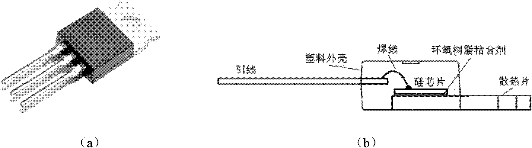
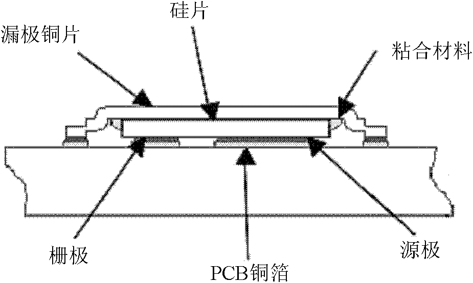
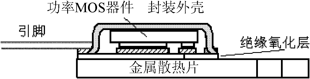
[0019] A low thermal resistance package structure for power MOS devices, such as image 3 As shown, it includes a power MOS device, a metal heat sink, a package shell, and external pins for the gate, source and drain. The surface of the metal heat sink has a thin layer of insulating oxide; the surface of the thin layer of insulating oxide has gate, source and drain metal pads corresponding to the gate, source and drain of the power MOS device, respectively; and the power MOS device Flip-chip on the thin insulating oxide surface of the metal heat sink; the gate, source and drain of the power MOS device are respectively welded to the gate, source and drain metal pads on the thin insulating oxide surface; thin The gate, source, and drain metal pads on the surface of the insulating oxide layer are connected to the external pins of the gate, source, and drain respectively; the package shell is installed outside the power MOS device to realize the isolation of the power MOS device fro...


PUM


Abstract

The invention discloses a low-heat-resistance packaging structure of a power MOS (Metal Oxide Semiconductor) device, belonging to the technical field of power semiconductor devices. In the invention, the silicon chip flip bridge clip technology and the conventional TO packaging technology are combined, and a flip heat-radiation structure is used so that the heat generated by the power MOS device directly flows to a metal heat sink, the problem of overhigh heat resistance caused by the conventional TO packaging of the power MOS device is solved; the large area contact of the bridge clip technology achieves the reduction of the heat resistance, the increment of the current capacity and the decrement of the parasitic inductance. The low heat resistance packaging structure of the power MOS device, provided by the invention, has the appearance of the conventional TO packaging; the power MOS device with excellent performance is packaged without adding the packaging equipment, but only properly increasing the related equipment of the bridge clip and the flip technique. The low heat resistance packaging structure of the power MOS device, provided by the invention, has about 80% of reducedheat resistance, about two times of increased current capacity and largely reduced parasitic inductance compared with the conventional TO packaging structure through the proving of the actual testing.

Description

Technical field [0001] The invention belongs to the technical field of power semiconductor devices, and relates to a packaging structure of a power MOS device. Background technique [0002] The encapsulation of power semiconductor devices usually refers to the installation of housings for semiconductor devices on silicon wafers. It not only protects the chip and enhances thermal conductivity, but also serves as a bridge between the internal world of the chip and the external circuit and the general function of specifications. The main function of the package is to provide physical protection and electrical connection for the chip, while realizing the standardization and standardization of semiconductor devices or integrated circuits. [0003] Because the chip must be isolated from the outside world, in order to prevent the impurities in the air from corroding the chip circuit and causing electrical performance degradation, protect the chip surface and connecting leads, etc., so tha...

Claims


Application Information

Patent Timeline
Patent Type & Authority Applications(China)
IPC IPC(8): H01L29/78H01L23/31H01L23/367
CPCH01L2224/73253H01L2924/0002H01L2224/48091H01L2224/73265H01L2224/32245H01L2224/48247H01L2924/13091
Inventor 陈勇赵建明夏建新
Owner 广东成利泰科技有限公司
Why Eureka
Try Eureka