Substrate for flexible luminous device and preparation method thereof

A light-emitting device and substrate technology, which is applied in the manufacture of semiconductor/solid-state devices, electric solid-state devices, semiconductor devices, etc., can solve the problems of high square resistance, poor bonding force between carbon nanotubes and flexible substrates, and smooth surface of thin-layer carbon nanotubes Degree difference etc.

Inactive Publication Date: 2011-10-05
UNIV OF ELECTRONICS SCI & TECH OF CHINA
View PDF2 Cites 11 Cited by
  • Summary
  • Abstract
  • Description
  • Claims
  • Application Information

AI Technical Summary

Problems solved by technology

[0008] The technical problem to be solved by the present invention is how to provide a substrate for a flexible light-emitting device and its preparation method. The problem of poor force improves the conductivity of thin-layer carbon nanotubes and the barrier ability of the substrate to water and oxygen

Method used


Image

  • Substrate for flexible luminous device and preparation method thereof
  • Substrate for flexible luminous device and preparation method thereof
  • Substrate for flexible luminous device and preparation method thereof

Examples


Embodiment 1

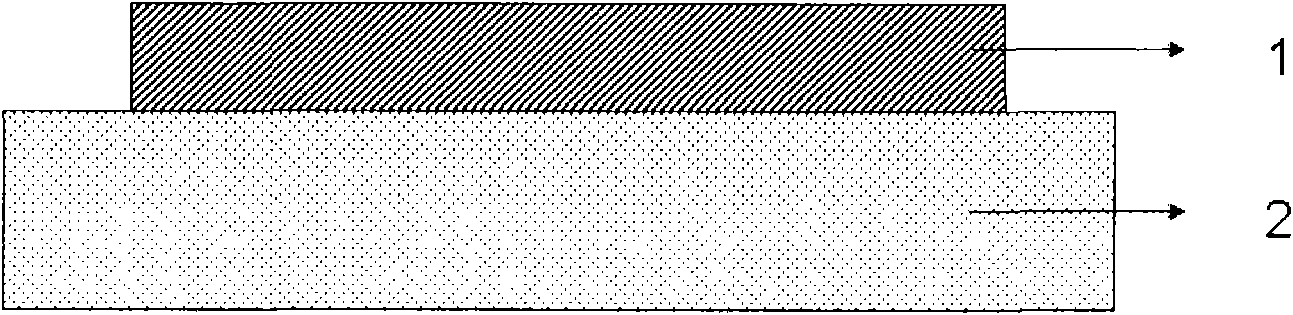
[0100] Such as figure 1 As shown in the substrate structure, the flexible substrate 1 uses an adhesive that requires double curing, and the conductive layer 2 uses carbon nanotubes. The gaps in the carbon nanotube layer are filled with inorganic luminescent nanoparticles, and the size of the inorganic luminescent nanoparticles is 15 nanometers. The thickness of the carbon nanotube layer is 70nm.

[0101] The preparation method is as follows:

[0102] ① Clean the glass substrate with surface roughness less than 1nm, and dry it with dry nitrogen after cleaning;

[0103] ② Evenly disperse carbon nanotubes in a solvent, and prepare a carbon nanotube layer on a clean substrate by spin coating. The rotation speed of spin coating is 4000 rpm, the duration is 60 seconds, and the film thickness is about 70 nanometers;

[0104] ③ Drop-coat the solution containing inorganic luminescent nanoparticles on the carbon nanotube layer, place the glass substrate in an environment of 80°C for 3...

Embodiment 2

[0112] Such as figure 1 In the substrate structure shown, the flexible substrate 1 uses an adhesive that requires double curing, the conductive layer 2 uses carbon nanotubes, and the gaps in the carbon nanotube layer are filled with inorganic luminescent nanoparticles, and the size of the inorganic luminescent nanoparticles is 10 nanometers. The thickness of the carbon nanotube layer is 60nm, and the adhesive raw material comprises the following components:

[0113]

[0114] The preparation method is similar to Example 1.

Embodiment 3

[0116] Such as figure 1 As shown in the substrate structure, the flexible substrate 1 uses an adhesive that requires double curing, the conductive layer 2 uses carbon nanotubes, and the gaps in the carbon nanotube layer are filled with inorganic luminescent nanoparticles, and the size of the inorganic luminescent nanoparticles is 5 nanometers. The thickness of the carbon nanotube layer is 50nm, and the adhesive raw material comprises the following components:

[0117]

[0118]

[0119] The preparation method is similar to Example 1.


PUM

PropertyMeasurementUnit
thicknessaaaaaaaaaa
sizeaaaaaaaaaa
surface roughnessaaaaaaaaaa

Abstract

The invention discloses a substrate for a flexible luminous device. The substrate comprises a flexible substrate and a conductive layer, and the flexible substrate and the conductive layer are formed in one of the following two modes: (1) the flexible substrate is adhesive to be doubly cured, the conductive layer is a thin layer carbon nano tube, and inorganic luminous nano particles are filled into gaps of the thin layer carbon nano tube; and (2) the flexible substrate is inorganic luminous nano particle-doped adhesive to be doubly cured, the conductive layer is a thin layer carbon nano tube, and the inorganic luminous nano particle-doped adhesive to be doubly cured is filled into gaps of the thin layer carbon nano tube, wherein the adhesive to be doubly cured comprises an ultraviolet curing and thermal curing system, an ultraviolet curing and microwave curing system, an ultraviolet curing and anaerobic curing system and an ultraviolet curing and electron beam curing system.

Description

technical field [0001] The invention relates to the technical field of organic optoelectronics, in particular to a substrate for a flexible light-emitting device and a preparation method thereof. Background technique [0002] Optoelectronics technology is a rapidly developing industry with high technological content after microelectronics technology. With the rapid development of optoelectronic technology, optoelectronic products such as solar cells, optical image sensors, flat panel displays, and thin film transistors have gradually matured, and they have greatly improved people's lives. At the same time, the wide application of optoelectronic information technology in various fields of social life has also created a huge growing market. Developed countries regard the optoelectronic information industry as one of the key development areas, and the competition in the optoelectronic information field is unfolding worldwide. [0003] Optoelectronics technology is a rapidly d...

Claims


Application Information

Patent Timeline
Patent Type & Authority Applications(China)
IPC IPC(8): H01L51/52H01L51/54C09J4/02C09J167/06C09J4/00C09J163/00H01L51/56
Inventor 于军胜李璐马柱蒋亚东
Owner UNIV OF ELECTRONICS SCI & TECH OF CHINA
Why Eureka
Try Eureka