Method for growing indium arsenide/indium gallium arsenide quantum well material on indium phosphide substrate

A technology of indium arsenide and indium phosphide, which is applied in the field of semiconductor laser manufacturing, can solve the problems of volatile InAs quantum well materials, quality of defective materials, degradation and the like

Active Publication Date: 2011-10-05
INST OF SEMICONDUCTORS - CHINESE ACAD OF SCI
View PDF3 Cites 9 Cited by
  • Summary
  • Abstract
  • Description
  • Claims
  • Application Information

AI Technical Summary

Problems solved by technology

The use of MOCVD technology to grow InAs/InGaAs quantum well materials in the 2μm band requires attention to the following two issues: 1. InAs quantum well materials are easy to volatilize at high temperatures, so they need to be grown in a suitable temperature window (460°C-500°C); 2. .The strain of InAs quantum well

Method used


Image

  • Method for growing indium arsenide/indium gallium arsenide quantum well material on indium phosphide substrate
  • Method for growing indium arsenide/indium gallium arsenide quantum well material on indium phosphide substrate
  • Method for growing indium arsenide/indium gallium arsenide quantum well material on indium phosphide substrate

Examples


Embodiment

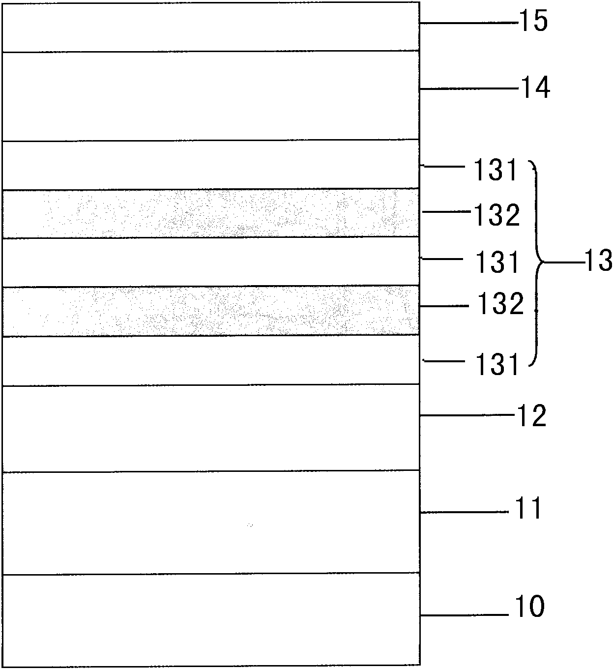
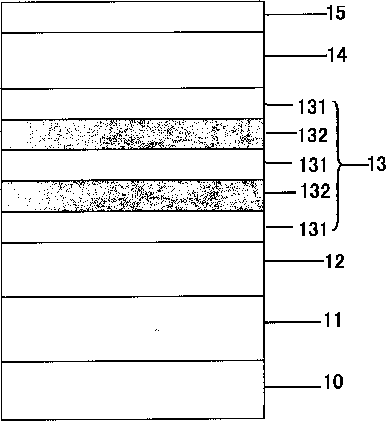
[0032] see again figure 1 As shown, a method of growing indium arsenide / indium gallium arsenide quantum well material on an indium phosphide substrate of the present invention comprises the following steps:

[0033] Step 1: select a half-insulated InP single wafer as the substrate 10;

[0034] Step 2: Using the metal organic compound vapor deposition method, a buffer layer 11, a lower waveguide layer 12, a double quantum well structure 13, an upper waveguide layer 14 and a capping layer 15 are sequentially grown on the substrate 10, and the indium phosphide layer is completed. Fabrication of indium arsenide / indium gallium arsenide quantum well materials grown on substrates.

[0035] The buffer layer 11 is an intrinsic InP buffer layer with a deposition thickness of 200 nm and a growth temperature of 610° C.

[0036] The material of the lower waveguide layer 12 is In 0.72 Ga 0.28 As 0.61 P 0.39 , the wavelength corresponding to its band gap is 1.3 μm, its deposition thick...


PUM

PropertyMeasurementUnit
Deposition thicknessaaaaaaaaaa
Thicknessaaaaaaaaaa

Abstract

The invention discloses a method for growing indium arsenide/indium gallium arsenide quantum well material on an indium phosphide substrate. The method comprises the following steps of: 1, selecting the substrate; and 2, sequentially growing a buffer layer, a lower waveguide layer, a dual-quantum well structure, an upper waveguide layer and a cover layer to finish growing the indium arsenide/indium gallium arsenide quantum well material on the indium phosphide substrate. In the method, an InAs quantum well with a proper thickness is grown at relatively lower temperature to realize the functions of reducing shortcomings and increasing a transition wavelength to 2.3 mu m under high strain condition.

Description

technical field [0001] The invention belongs to the technical field of semiconductor laser manufacturing, and in particular relates to a method for growing indium arsenide / indium gallium arsenide quantum well materials on an indium phosphide substrate. Background technique [0002] Mid-infrared lasers with wavelengths longer than 2 μm have received great attention in the scientific research community due to their potential applications in gas detection. In 1994, using InAs as well, In 0.53 Ga 0.47 The quantum well structure with As barrier layer was used in 1.7μm mid-infrared laser for the first time. Since then, there have been many reports on InAs quantum well lasers, especially in the field of atmospheric detection in the 2 μm band. And with the improvement of MOCVD (metal organic compound vapor deposition) technology, the final commercial use of 2μm band lasers has a good foundation. The use of MOCVD technology to grow InAs / InGaAs quantum well materials in the 2μm ba...

Claims


Application Information

Patent Timeline
IPC IPC(8): H01S5/343
Inventor 汪明杨涛
Owner INST OF SEMICONDUCTORS - CHINESE ACAD OF SCI
Why Eureka
Try Eureka