Method for manufacturing current blocking layer of gallium nitride-based light-emitting diode (LED)
A technology of current blocking layer and light emitting diode, which is applied in circuits, electrical components, semiconductor devices, etc., can solve the problems of high production cost and complex process.
- Summary
- Abstract
- Description
- Claims
- Application Information
AI Technical Summary
Problems solved by technology
Method used
Image
Examples
Embodiment
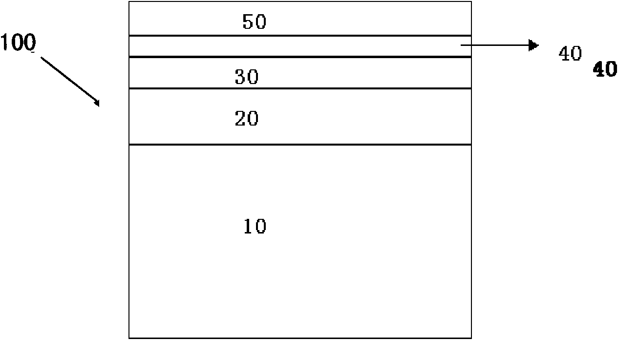
[0028] see again Figure 1 to Figure 4 As shown, the present invention provides a method for preparing a gallium nitride-based light-emitting diode current blocking layer, comprising the following steps:
[0029] Step 1: Take a GaN LED epitaxial wafer 100, which is composed of a sapphire substrate 10, N-type GaN 20, multiple quantum wells 30, AlGaN EBL 40 and P-type GaN 50 ( figure 1 middle);
[0030] Step 2: Isolating the gallium nitride LED epitaxial wafer 100 into square repeating units 101 with a size of 1000×1000um, each unit 101 is an independent LED chip;
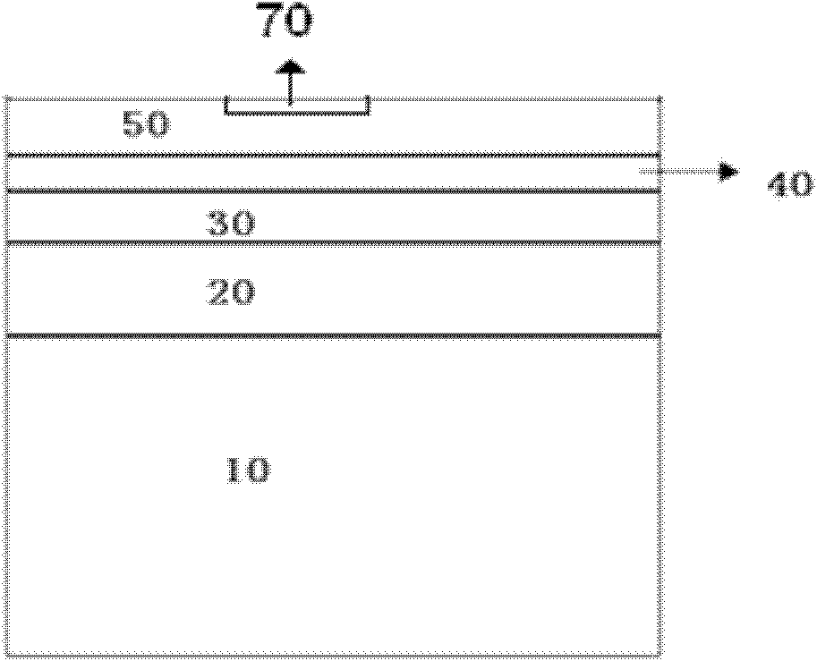
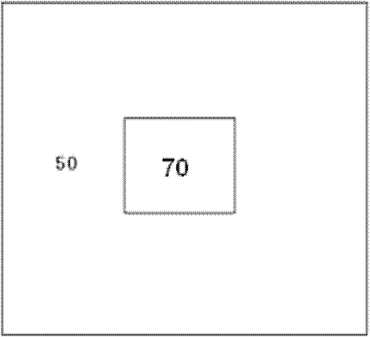
[0031] Step 3: Perform silicon ion implantation on the central 100×100um area of the upper surface of the unit 101 and form the current blocking layer 70 ( figure 2 or image 3 middle);
[0032] Step 4: Deposit a NiAgNiAu metal film on the entire upper surface of the unit 101 as the P electrode 60 ( Figure 4 Middle), the P electrode 60 covers the entire current blocking layer 70 .
PUM
 Abstract
Description
Claims
Application Information
 - R&D
- Intellectual Property
- Life Sciences
- Materials
- Tech Scout
- Unparalleled Data Quality
- Higher Quality Content
- 60% Fewer Hallucinations
Browse by: Latest US Patents, China's latest patents, Technical Efficacy Thesaurus, Application Domain, Technology Topic, Popular Technical Reports.
© 2025 PatSnap. All rights reserved.Legal|Privacy policy|Modern Slavery Act Transparency Statement|Sitemap|About US| Contact US: help@patsnap.com


