Manufacturing process of high-density printed board with holes in pads

A processing technology and hole-in-disk technology, which is applied in the field of PCB manufacturing, can solve problems such as virtual welding or poor welding, and achieve the effect of improving quality, avoiding poor contact and virtual welding, and high-density packaging and connection.

Active Publication Date: 2011-10-12
SHENZHEN BOMIN ELECTRONICS
View PDF3 Cites 22 Cited by
  • Summary
  • Abstract
  • Description
  • Claims
  • Application Information

AI Technical Summary

Problems solved by technology

[0005] In order to solve the existing problem that the through holes and pads on the PCB board are stacked and stacked to match and connect with BGA packaged devices, the problem of easy occurrence of virtual soldering or poor soldering exists, and the purpose of the present invention is to provide a hole in the tape reel High-density printed board processing technology

Method used


Image

  • Manufacturing process of high-density printed board with holes in pads
  • Manufacturing process of high-density printed board with holes in pads
  • Manufacturing process of high-density printed board with holes in pads

Examples


Embodiment Construction
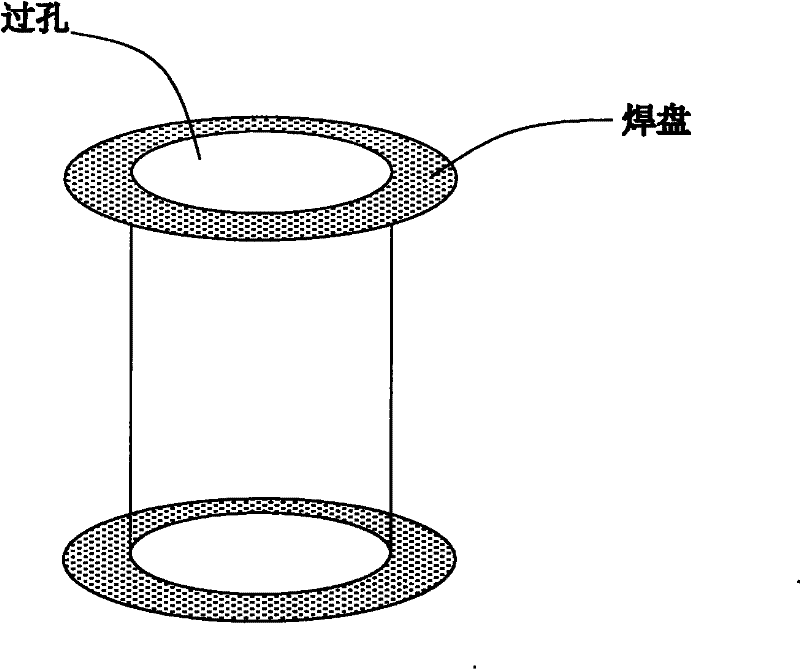
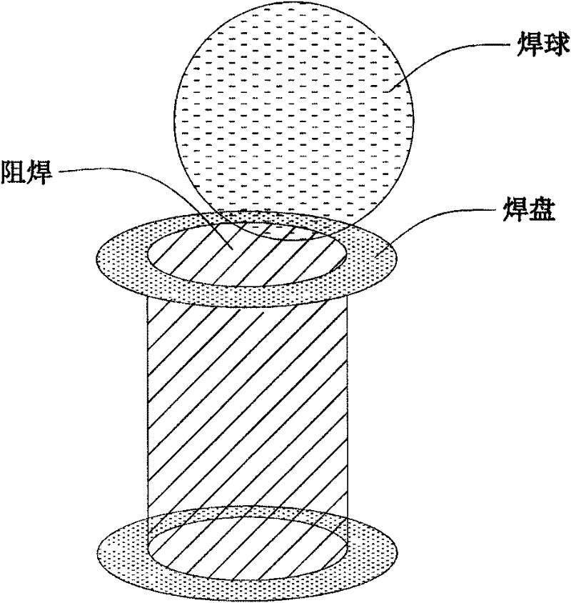
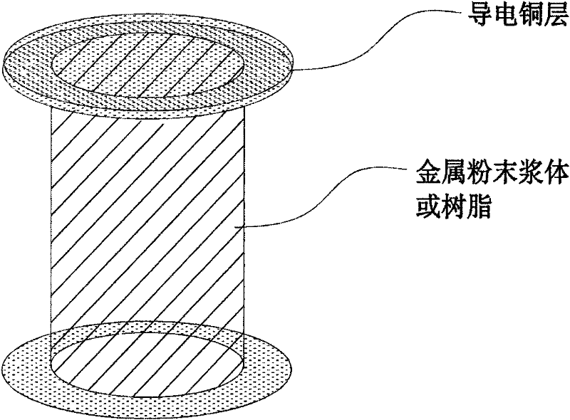
[0031] The core idea of ​​the present invention is: by filling the slurry in the annular disc hole formed in the circuit board pad, the disc hole in the pad is filled to form a solid body, and the entire circuit board is welded by grinding. The slurry filled in the hole in the disk is flat and forms the same plane as the adjacent conductor surface, and then the circuit board is metallized and electroplated so that the upper and lower surfaces of the hole filled with the slurry are covered with a layer of conductive copper Layer, when the array solder balls or pins at the bottom of the BGA package device are connected to the pads of the above-mentioned holes in the pad, it can ensure sufficient contact with the pads and avoid the problems of weak soldering and virtual soldering.

[0032] In order to illustrate the idea and purpose of the present invention, the present invention will be further described below in conjunction with the accompanying drawings and specific embodiments...


PUM


Abstract

The invention discloses a manufacturing process of a high-density printed board with holes in pads. The process is characterized by comprising the following steps: filling slurry in holes in pads formed in a welding plate of a circuit board, filling the holes in pads in the welding plate completely to form a solid body is formed; polishing, thus the slurry filled in the holes in pads on the welding plate of the whole circuit board is smooth, and forming the same plane with the adjacent conductor surface; and carrying out hole metallization and electroplating on hole walls of other non-holes in pads on the circuit board, thus a conductive copper layer is coated on the upper surface and the lower surface of the holes in pads filled with the slurry. When array welded balls or QFP (quad flat pack) pins and the like at the bottom part of a U-BGA (ball grid array) package appliance are connected with the welding plate of the holes in pads, the full contact with the welding plate can be ensured, and the problems of nonfarm welding and insufficient welding can be prevented form occurring.

Description

technical field [0001] The invention relates to PCB manufacturing technology, in particular to a processing technology of a high-density printed board with holes in a reel. Background technique [0002] With the advancement of electronic technology, the integration level of chips has been continuously improved, the number of I / O pins has increased sharply, and the power consumption has also increased accordingly, and the requirements for integrated circuit packaging have become more stringent. In order to meet the needs of development, U-BGA packaging began to be used in production. U-BGA (Ball Grid Array) is a ball grid array packaging technology, also known as high-density surface chip-scale packaging technology, which is mainly used in An array of solder balls is made on the bottom of the package substrate as an I / O terminal of the circuit to interconnect with a printed circuit board (PCB). [0003] The current connection between printed circuit boards and BGA packaged d...

Claims


Application Information

Patent Timeline
Patent Type & Authority Applications(China)
IPC IPC(8): H05K3/42
Inventor 黄建国
Owner SHENZHEN BOMIN ELECTRONICS
Why Eureka
Try Eureka