Manufacturing method of shallow trench isolation

A manufacturing method and technology of shallow trenches, applied in semiconductor/solid-state device manufacturing, electrical components, circuits, etc., can solve the problems of high cost, low cost-efficiency ratio, and complicated process steps, so as to reduce process cost and realize smoothness The effect of simplifying and simplifying the process steps

Active Publication Date: 2011-10-19
SEMICON MFG INT (SHANGHAI) CORP +1
View PDF6 Cites 10 Cited by
  • Summary
  • Abstract
  • Description
  • Claims
  • Application Information

AI Technical Summary

Problems solved by technology

[0010] In the existing shallow trench isolation manufacturing method, in order to smooth the corners of the shallow trench and obtain sufficient smoothness, two layers of oxide layers are formed on the sidewall and bottom of the trench, and three oxidation processes are carried out successively. The process steps are relatively complex
Among them, the process of forming the liner oxide layer 201 and the sacrificial oxide layer 202 using the in-situ steam generation process ISSG is relatively expensive due to equipment and raw material limitations, and the cost-effectiveness is not high.

Method used


Image

  • Manufacturing method of shallow trench isolation
  • Manufacturing method of shallow trench isolation
  • Manufacturing method of shallow trench isolation

Examples


no. 1 example

[0039] Figure 8 to Figure 15 It is a process schematic diagram of the first embodiment of the method of the present invention. The manufacturing method of this embodiment will be described in detail in conjunction with the accompanying drawings.

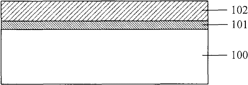
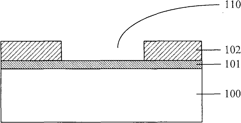
[0040] Such as Figure 8As shown, firstly, a semiconductor substrate 300 is provided, and the semiconductor substrate 300 is covered with a mask structure 301 . The mask structure 301 may be a single layer of silicon oxide layer, silicon nitride layer or polysilicon layer or a stack structure of any combination, and may also be a stack structure of a dielectric layer and a mask layer stacked in sequence. When the dielectric layer is used to form openings in the photolithography mask structure 301 , it plays the role of etching stop and protecting the semiconductor substrate 300 . The thickness of the mask structure 301 may be 100 nm to 120 nm. In this embodiment, the semiconductor substrate 300 is made of polysilicon, and the ma...

no. 2 example

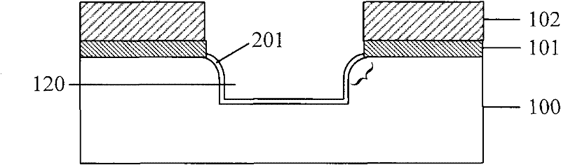
[0051] In the first embodiment, the second liner oxide layer 303 is regenerated on the sidewall and bottom surface of the annealed trench 320 to weaken the internal stress of the oxide layer, and the stress acts on the corners of the top of the trench 320 , may cause adverse effects. In order to further simplify the process, this embodiment also provides an optional method. After the step of removing the mask structure 301, a sacrificial oxide layer is formed on the surface of the exposed semiconductor substrate to improve the uniformity of silicon oxide on the corner surface. In order to weaken the adverse effect of the internal stress of the liner oxide layer 302 on the corners. The difference between this embodiment and the first embodiment lies in the step of forming the sacrificial oxide layer. Thus, in Figure 12 The process before the annealing step shown is completely the same as that of the first embodiment, and will not be repeated here.

[0052] Such as Figure ...


PUM

PropertyMeasurementUnit
Thicknessaaaaaaaaaa
Thicknessaaaaaaaaaa
Thicknessaaaaaaaaaa

Abstract

The invention provides a manufacturing method of shallow trench isolation, which comprises the steps of: providing a semiconductor substrate with a masking structure covered on a surface, wherein an opening for exposing the semiconductor substrate is formed on the masking structure; etching a trench corresponding to the opening on the semiconductor substrate by taking the masking structure as a mask; forming lining oxidizing layers on sidewalls and the bottom of the trench; annealing under an argon atmosphere; and filling an insulating medium in the trench to form the shallow trench isolation. The manufacturing method provided by the invention can ensure that corners on the top of the trench are smoothened; and in addition, compared with the prior art, the manufacturing method has the advantages of simplifying process steps and lowering process cost.

Description

technical field [0001] The invention relates to a semiconductor manufacturing process, in particular to a shallow trench manufacturing method. Background technique [0002] With the advancement of semiconductor manufacturing technology, shallow trench isolation (STI, Shallow Trench Isolation) method has gradually replaced other isolation methods such as local silicon oxidation method used in traditional semiconductor device manufacturing. Compared with other isolation methods, the shallow trench isolation method has many advantages, mainly including: 1. The STI method can obtain a narrower semiconductor device isolation width, thereby increasing the device density; 2. The STI method can improve the surface flatness, so it can be used in Effectively control the minimum line width during lithography. [0003] It is found in the existing process that the smoothness of the corners of shallow trenches used in shallow trench isolation has a strong correlation with leakage. The sm...

Claims


Application Information

Patent Timeline
IPC IPC(8): H01L21/762
Inventor 陈碧钦宋化龙沈忆华
Owner SEMICON MFG INT (SHANGHAI) CORP
Why Eureka
Try Eureka