Vertical double-diffused metal oxide semiconductor power device with super junction structure

An oxide semiconductor, vertical double diffusion technology, applied in the direction of semiconductor devices, electrical components, circuits, etc., can solve the problems of inaccessibility, drop in breakdown voltage, insufficient breakdown voltage, etc., to improve performance and improve breakdown voltage. Effect

Inactive Publication Date: 2011-11-02
ZHEJIANG UNIV
View PDF3 Cites 16 Cited by
  • Summary
  • Abstract
  • Description
  • Claims
  • Application Information

AI Technical Summary

Problems solved by technology

[0005] However, in the current actual technology, due to the existence of an N+ substrate depletion effect, it will affect the output of the electric field distribution, making it impossible to achieve Figure 4 The ideal uniform electric field shown, that is, the ideal breakdown voltage cannot be achieved; specifically, it will be at the junction of the bottom of the P-type columnar region and the N-type epitaxy ( image 3 middle part b) produces an electric field peak value, so that the breakdown voltage will be lower than the ideal situation; the electric field distribution of the current technology is as follows Figure 5 As shown, the area of ​​the shaded part of the electric field in the figure is relatively Figure 4 decreases, indicating that the breakdown voltage is insufficient

Method used


Image

  • Vertical double-diffused metal oxide semiconductor power device with super junction structure
  • Vertical double-diffused metal oxide semiconductor power device with super junction structure
  • Vertical double-diffused metal oxide semiconductor power device with super junction structure

Examples


Embodiment Construction

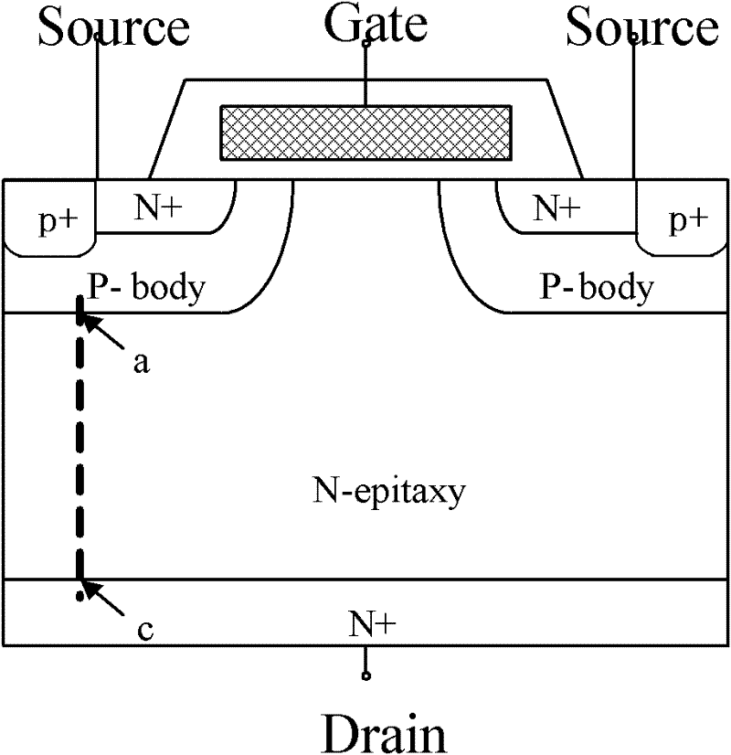
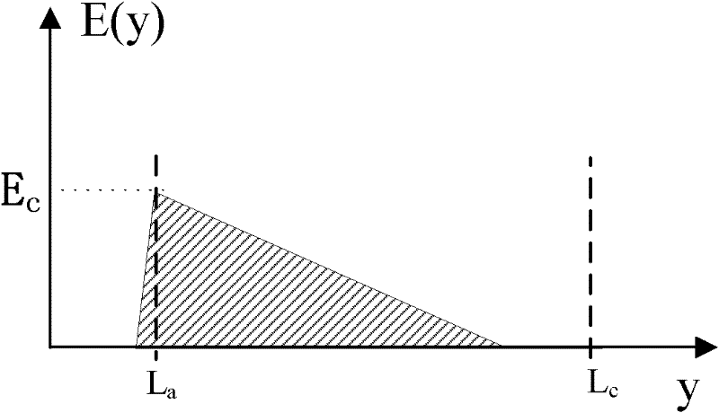
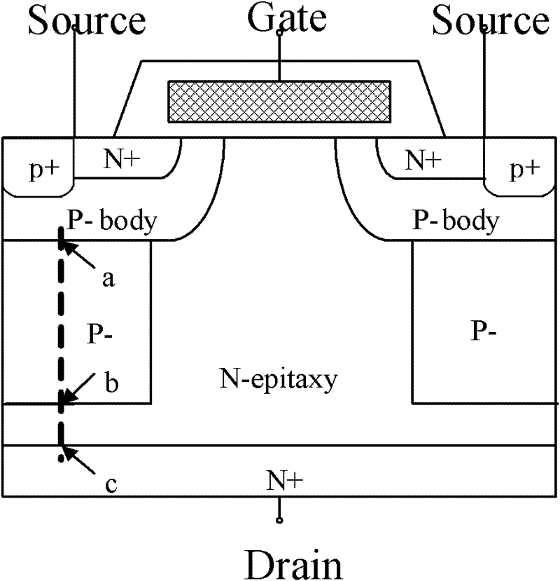
[0038] like Image 6 As shown, a vertical double-diffused metal oxide semiconductor power device with a superjunction structure, including a cell region I, a transition region II surrounding the cell region, and a terminal region III surrounding the transition region;

[0039] Metal layer I10 and metal layer II15 are provided at the bottom and top of the cell region I, the transition region II and the terminal region III, and an n-type doped semiconductor material substrate 1 is arranged on the bottom metal layer I10, and the n-type doped semiconductor material substrate 1 is provided with an n-type doped semiconductor material drift layer 2, and an n-type doped semiconductor material drift layer 2 is provided with a discontinuous p-type doped columnar semiconductor region 3;

[0040] A p-type doped semiconductor region 14 is provided on the p-type doped columnar semiconductor region 3 in the cell region 1, and the p-type doped semiconductor region 14 is located in the n-type ...


PUM


Abstract

The invention relates to the technical field of semiconductor devices, in particular to a vertical double-diffused metal oxide semiconductor power device with a super junction structure. The vertical double-diffused metal oxide semiconductor power device comprises a cell region I, a transition region II and a terminal region III, wherein the transition region II surrounds the cell region, and the terminal region III surrounds the transition region. The vertical double-diffused metal oxide semiconductor power device is characterized in that an insulating medium material is arranged at the bottom of a second conduction type cylindrical semiconductor region in the cell region I. The invention has the beneficial effects that the distribution of an electric field is close to ideal uniform distribution, a breakdown voltage of a practical super junction structure device is increased and performances of the device are further improved according to the vertical double-diffused metal oxide semiconductor power device with the improved super junction structure.

Description

technical field [0001] The invention relates to the technical field of semiconductor devices, in particular to a vertical double-diffused metal oxide semiconductor power device with a superjunction structure. Background technique [0002] At present, power devices are widely used in switching power supply, automotive electronics, industrial control and other fields; vertical double-diffused metal oxide semiconductor field effect transistor (Vertical Double-diffused MOSFET, referred to as VDMOS), compared with traditional bipolar power transistors, has Many excellent properties, such as high input impedance, fast switching speed, high operating frequency, good voltage control, good thermal stability, no secondary breakdown, etc., are relatively excellent power devices. Especially the invention of super junction structure VDMOS, which overcomes the contradiction between on-resistance and breakdown voltage of traditional power VDMOS; it changes the structure of traditional powe...

Claims


Application Information

Patent Timeline
Patent Type & Authority Applications(China)
IPC IPC(8): H01L29/78H01L29/06
Inventor 胡佳贤韩雁张世峰张斌
Owner ZHEJIANG UNIV
Why Eureka
Try Eureka