Semiconductor device and method for forming same

A semiconductor and device technology, applied in the field of semiconductor devices and their formation, can solve the problems of device performance degradation, band-band leakage current and source-drain junction capacitance increase, etc., to improve performance, avoid steepness reduction, and avoid ion diffusion. Effect

Active Publication Date: 2011-11-09
INST OF MICROELECTRONICS CHINESE ACAD OF SCI
View PDF4 Cites 6 Cited by
  • Summary
  • Abstract
  • Description
  • Claims
  • Application Information

AI Technical Summary

Problems solved by technology

Since the formation of inverted doped wells in the substrate usually improperly introduces dopants into the source and drain regions, the inverted doped well distribution overlaps with the doping of the source / drain regions, causing band- Increased band leakage current and source-drain junction capacitance, resulting in degraded device performance

Method used


Image

  • Semiconductor device and method for forming same
  • Semiconductor device and method for forming same
  • Semiconductor device and method for forming same

Examples


Embodiment Construction

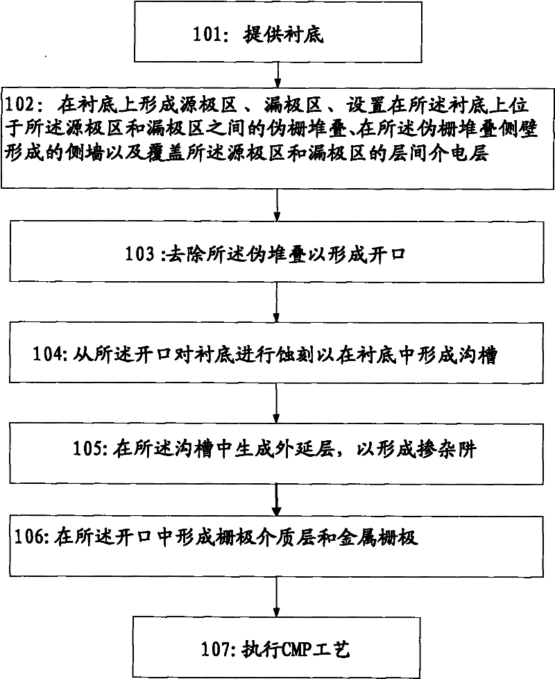
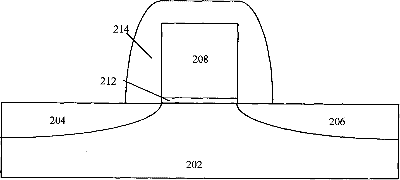
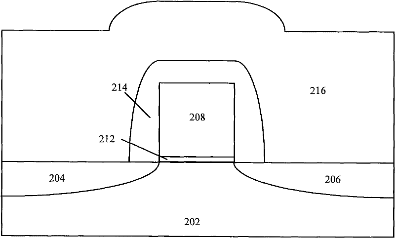
[0010] The invention generally relates to a manufacturing method of a semiconductor device, in particular to a semiconductor device and a method for forming a doped well by using an in-situ doping process. The following disclosure provides many different embodiments or examples for implementing different structures of the present invention. To simplify the disclosure of the present invention, components and arrangements of specific examples are described below. Of course, they are only examples and are not intended to limit the invention. Furthermore, the present invention may repeat reference numerals and / or letters in different instances. This repetition is for the purpose of simplicity and clarity and does not in itself indicate a relationship between the various embodiments and / or arrangements discussed. In addition, various specific process and material examples are provided herein, but one of ordinary skill in the art may recognize the applicability of other processes ...


PUM

PropertyMeasurementUnit
Thicknessaaaaaaaaaa
Thicknessaaaaaaaaaa
Depthaaaaaaaaaa

Abstract

The invention relates to a method for making a semiconductor device. The method comprises the following steps of: removing pseudo stack to form an opening; etching a substrate from the opening to form a groove; generating an epitaxial layer in the groove by using an epitaxial growth process to form a doped pit; and forming a grid dielectric layer and a metal grid in the opening. By the method, the problems that in the conventional method, the steepness of the doped pit formed by utilizing ion implantation and annealing is reduced and a doping agent is incorrect led to a source electrode area and a drain electrode area are solved so as to improve the performance of the device.

Description

technical field [0001] The present invention generally relates to a semiconductor device and a method of forming the same. More specifically, it relates to a semiconductor device and a method for forming a doped well by using an in-situ doping process. Background technique [0002] With the development of the semiconductor industry, integrated circuits with higher performance and more functions require greater component density, and the size, size and space of each component, between components, or each component itself needs to be further reduced. Correspondingly, in order to improve the performance of the MOSFET (Metal Oxide Semiconductor Field Effect Transistor) device, it is necessary to further reduce the gate length of the MOSFET device. However, as the gate length continues to decrease, the width of the depletion layer close to the source and drain, for example, less than 40nm, will produce a more serious short channel effect (short channel effect or SCE for short), ...

Claims


Application Information

Patent Timeline
IPC IPC(8): H01L21/336H01L29/78H01L29/423H01L29/10
Inventor 尹海洲朱慧珑骆志炯
Owner INST OF MICROELECTRONICS CHINESE ACAD OF SCI
Why Eureka
Try Eureka