High heat radiation LED (Light Emitting Diode) nonmetal substrate and high heat radiation LED element as well as making method thereof

A non-metallic plate and non-metallic technology, which is applied in the field of LED non-metallic substrate manufacturing method, can solve the problems of inability to apply LED chip packaging, reduced area of ​​bonding die pad, small precision, etc.

Inactive Publication Date: 2011-11-09
陈 一璋
View PDF4 Cites 14 Cited by
  • Summary
  • Abstract
  • Description
  • Claims
  • Application Information

AI Technical Summary

Problems solved by technology

Furthermore, the current structure of the heat dissipation substrate is still challenged. The reason is that the size of the LED chip is becoming smaller and smaller, so the area of ​​the die-bonding pad is relatively reduced, and the manufacturing method of the heat-conducting copper pillar has a certain size limit, which cannot be applied to the miniaturization of the LED chip. Packaging, and the use of sputtered copper foil also has its minimum precision limit. In terms of through-holes for electrical connection, a 1mm thick ceramic board must be pierced with a through-hole with an aperture of 0.5mm to form a conductive hole

Method used


Image

  • High heat radiation LED (Light Emitting Diode) nonmetal substrate and high heat radiation LED element as well as making method thereof
  • High heat radiation LED (Light Emitting Diode) nonmetal substrate and high heat radiation LED element as well as making method thereof
  • High heat radiation LED (Light Emitting Diode) nonmetal substrate and high heat radiation LED element as well as making method thereof

Examples


Embodiment Construction

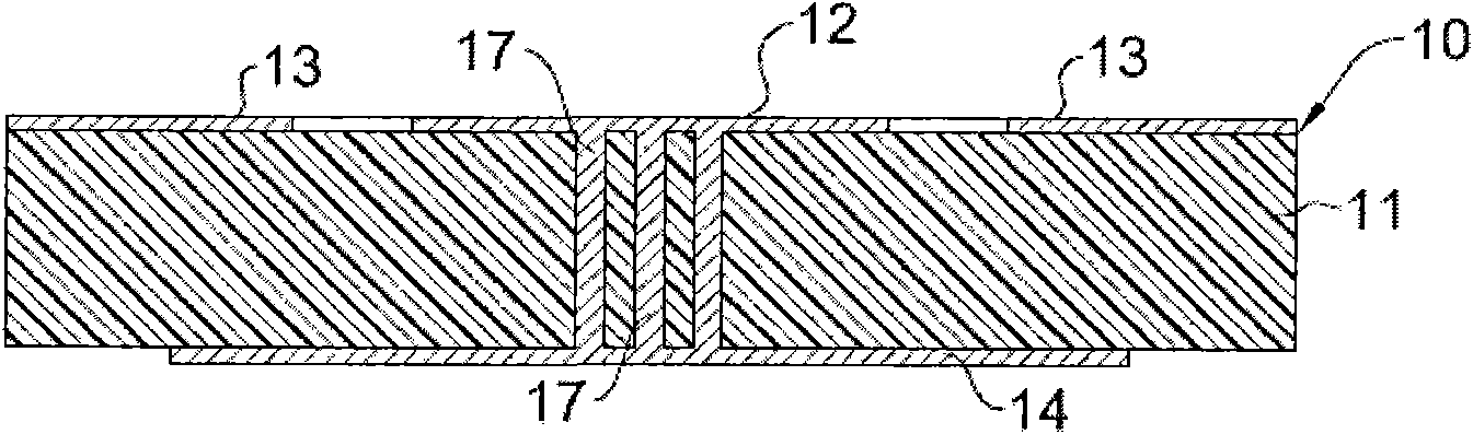
[0052] See first Figures 1A to 1EAs shown, it is a production flow chart of the first preferred embodiment of a high heat dissipation LED element of the present invention. In this embodiment, the high heat dissipation LED element is used to be welded on the heat dissipation module 40, as Figure 8A As shown, it contains:

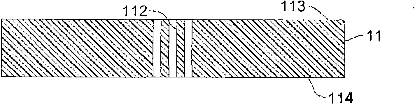
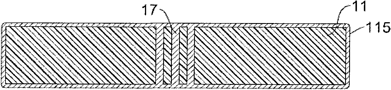
[0053] Provide a non-metallic plate body 11; in this embodiment, the non-metallic plate body 11 is a ceramic plate body, also can be a silicon substrate, its thickness is 0.3mm to 2mm;

[0054] At least one second through hole 112 is formed on the non-metallic plate body 11; in this embodiment, each second through hole 112 is formed by laser drilling or other drilling processing methods, and its diameter is more than 0.02 mm;

[0055] Electroplating the outer surface of the non-metal plate body 11 and each second through hole 112, and forming an electroplated copper layer 115 on the outer surface, and forming a solid thermally conductive copper column 17 i...


PUM

PropertyMeasurementUnit
thicknessaaaaaaaaaa
pore sizeaaaaaaaaaa
pore sizeaaaaaaaaaa

Abstract

The invention relates to a high heat radiation LED (Light Emitting Diode) nonmetal substrate and a high heat radiation LED element as well as a making method thereof. The making method mainly comprises the following steps: at least one through hole is pre-molded in a crystal bonding region of a nonmetal plate body; in coordination with the copper layer electroplating step, an electroplating copper layer is coated on the external surface of the nonmetal plate body; a solid heat conducting copper column is formed in the at least one through hole; the metal layer is patterned by using an etching technology; a crystal bonding pad and a wire bonding pad are formed on the upper surface of the ceramic plate body; a heat radiation pad is formed on the lower surface of the ceramic plate body corresponding to the crystal bonding pad so that the crystal bonding pad and the heat radiation pad are integrally molded with the heat conducting copper column; and the high heat can be rapidly conducted to the heat radiation pad of the lower surface through the heat conducting copper column while the crystal bonding pad reaches the high heat.

Description

technical field [0001] The invention relates to a method for manufacturing an LED non-metallic substrate, in particular to a high-radiation-radiation LED non-metal substrate and a method thereof, and a high-radiation-radiation LED component and a method thereof. Background technique [0002] Substrates used in LED chip packaging can be roughly divided into metal or non-metallic substrates such as ceramic substrates or silicon substrates. In terms of manufacturing methods for ceramic boards, there are currently four manufacturing methods, which are low-temperature co-fired multilayer ceramic boards ( LTCC) or a high-temperature co-fired multilayer ceramic board (HTCC), a direct bonded copper substrate (DBC) and a direct copper-plated substrate (DPC); among them, the thermal conductivity of the DBC and DPC substrates directly using ceramic boards is The best, but because the DBC substrate synthesizes the copper plate on the ceramic plate body, it must be completed in a high te...

Claims


Application Information

Patent Timeline
Patent Type & Authority Applications(China)
IPC IPC(8): H01L33/62H01L33/64H01L21/60H01L25/075
CPCH01L2224/48091H01L2924/09701H01L2224/49175
Inventor 陈一璋
Owner 陈 一璋
Why Eureka
Try Eureka