Current detection circuit

A current detection circuit and current technology, applied in the direction of circuit, measuring current/voltage, only measuring current, etc., can solve problems such as low withstand voltage, and achieve the effect of high-precision detection

Inactive Publication Date: 2011-11-16
PANASONIC CORP
View PDF1 Cites 24 Cited by
  • Summary
  • Abstract
  • Description
  • Claims
  • Application Information

AI Technical Summary

Problems solved by technology

However, even if LDD (Lightly Doped Drain) structure or the like is used to increase the withstand voltages between the drain-gate and the drain-substrate of the enhancement type MOSFET 137, in order to increase the mutual conduction between the source and the gate, the integrated The withstand voltage is usually the lowest in the circuit
Therefore, with respect to the minimum voltage value of the source voltage, a voltage equal to or less than the withstand voltage between the source and the gate can be applied to the gate of the enhancement type MOSFET 137 at most.

Method used


Image

  • Current detection circuit
  • Current detection circuit
  • Current detection circuit

Examples


no. 1 approach

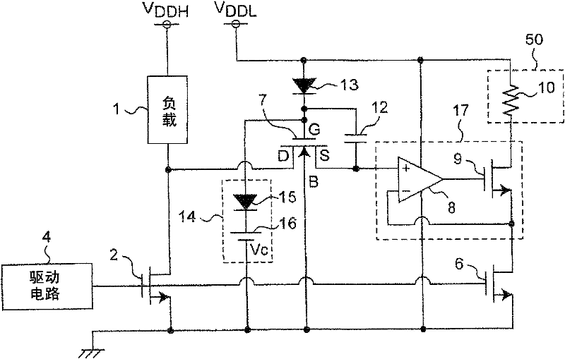
[0039] figure 1 It is a circuit diagram of the current detection circuit of the first embodiment of the present invention. in figure 1 In this embodiment, the current detection circuit of this embodiment is configured as an integrated circuit, and includes a load 1, a power transistor 2, a detection transistor 6, a voltage control circuit 17 including an operational amplifier 8 and an output transistor 9, a detection circuit 50 including a resistor 10, and a protection A MOSFET 7, a diode 13, an electrostatic capacitor 12, a clamping circuit 14 including a diode 15 and a DC voltage source 16, and a driving circuit 4 are used.

[0040] As described in detail later, the current detection circuit of this embodiment is characterized by having:

[0041] (a) The power transistor 2 has a source, a drain, and a gate, and controls the current flowing between the drain and the source by a control voltage applied to the gate;

[0042] (b) The detection transistor 6, which has a source, a dra...

no. 2 approach

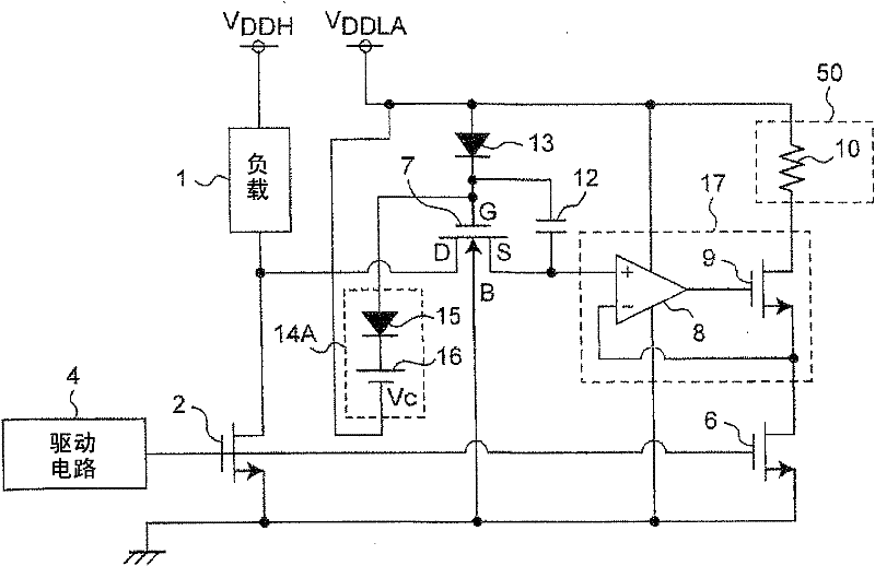
[0076] Figure 7 It is a circuit diagram of the current detection circuit of the second embodiment of the present invention. Compared with the first embodiment, this embodiment is different in that a load 1 is connected between the source of the power transistor 2 and the ground potential. In addition, the connection point between the drain of the power transistor 2 and the protection MOSFET 7 does not pass through the load 1, but is directly connected to the output power supply voltage V DDH Voltage source. in Figure 7 When the power transistor 2 is turned on by the drive circuit 4, the drain current flows through the power transistor 2 as in the first embodiment, and the resistance component of the power transistor 2 when it is turned on is more exciting than when it is not turned on. Drain voltage with low drain voltage. In addition, the voltage between the source and the drain of the power transistor 2 decreases, the potential difference between the drain and the gate of...


PUM


Abstract

The present invention provides a current detection circuit. Using a electrostatic capacitor (12) and a diode (13), a gate voltage of a protecting MOSFET (7) is increased when a drain voltage of a power transistor (2) increases. A voltage clamp circuit (14) clamps the maximum voltage of the gate voltage of the protecting MOSFET (7)to a predetermined clamp voltage (Vc). A voltage control circuit (17) controls a drain voltage of a sense transistor (6) so as to substantially coincide with a source voltage of the protecting MOSFET (7). A detection circuit (40) detects the current of the drain of the sense transistor (6). Therefore, even if the substrate bias effect occurs in the protecting MOSFET of the current detection circuit of the power transistor, the current of a load is detected precisely by means of a high voltage negatively fed back by the operation amplifier on the basis of satisfying the resistant voltage between the source and gate of the protecting MOSFET.

Description

Technical field [0001] The present invention relates to a current detection circuit for detecting the value of current flowing through a power semiconductor device. Background technique [0002] Power semiconductor devices such as thyristors (hereinafter referred to as power transistors) are semiconductors that convert and control electric power. For example, they are mostly used as drive elements for inverter control of motors or power for switching power supplies. control element. Specifically, in order to generate the driving torque of the motor load, the current flowing through the power transistor is used, and in the switching power supply, the power transistor is used for improving the responsiveness. In particular, compared with Bipolar Junction Transistor (BJT) or semiconductor thyristor, IGBT (Insulated Gate Bipolar Transistor: Insulated Gate Bipolar Transistor) and Power MOSFET (Metal Oxide Semiconductor Field Effect Transistor: Metal Oxide Semiconductor Field Effect T...

Claims


Application Information

Patent Timeline
Patent Type & Authority Applications(China)
IPC IPC(8): G01R19/00
CPCG01R19/0092H03K17/0822H03K2217/0027
Inventor 久米智宏
Owner PANASONIC CORP
Why Eureka
Try Eureka