Graphene/silicon pillar array Schottky junction photovoltaic cell and manufacturing method thereof

A Schottky junction, photovoltaic cell technology, applied in the field of solar cells, can solve the problems of energy loss, ineffective use of incident light energy, etc., and achieve the effects of small reflection coefficient, easy mass production, and improved efficiency

Inactive Publication Date: 2011-11-23
TSINGHUA UNIV
View PDF3 Cites 17 Cited by
  • Summary
  • Abstract
  • Description
  • Claims
  • Application Information

AI Technical Summary

Problems solved by technology

In the literature, the graphene / silicon Schottky junction adopts a planar structure, and the planar structure often cannot effectively utilize the incident light energy. For example, the reflectivity of planar silicon in the visible light range is as high as 30%, resulting in a large amount of energy loss.

Method used


Image

  • Graphene/silicon pillar array Schottky junction photovoltaic cell and manufacturing method thereof
  • Graphene/silicon pillar array Schottky junction photovoltaic cell and manufacturing method thereof
  • Graphene/silicon pillar array Schottky junction photovoltaic cell and manufacturing method thereof

Examples


Embodiment 1

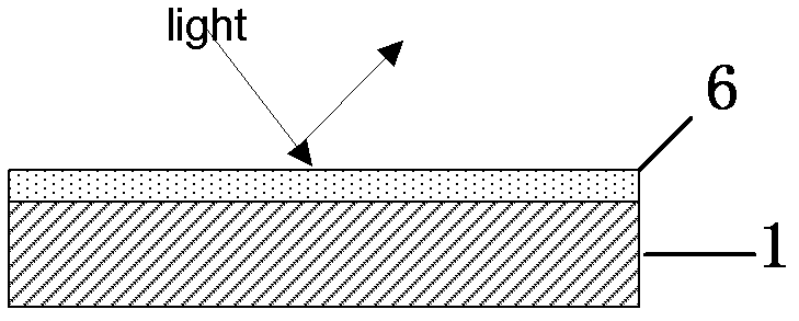
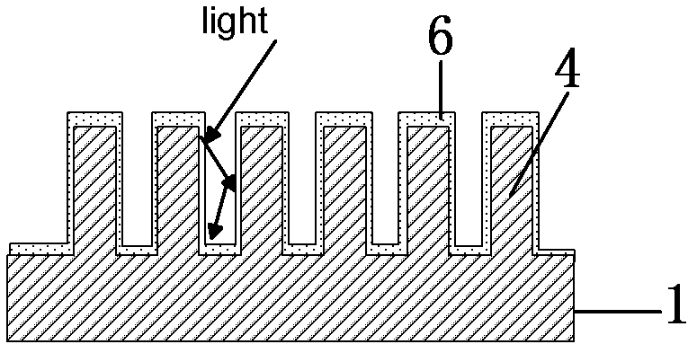
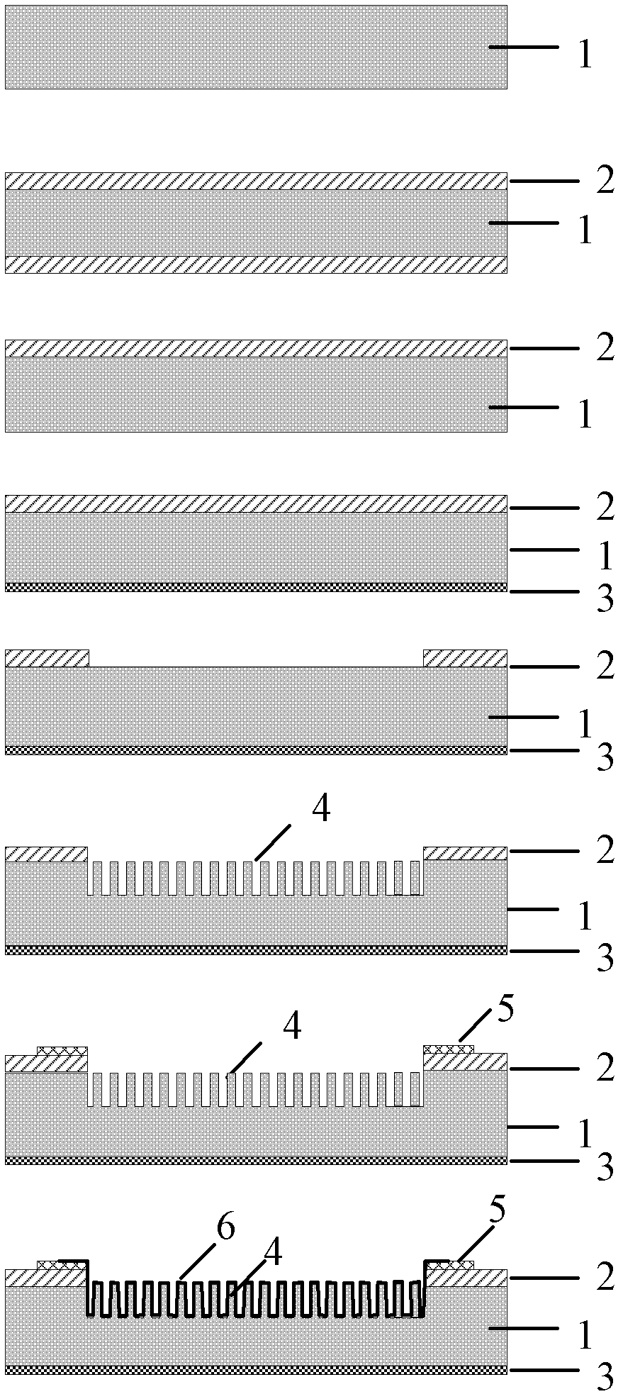
[0043] When the graphene / silicon column array Schottky junction photovoltaic cell is produced in this embodiment, the n-type (100) single crystal silicon substrate 1 with a resistivity of 2-3Ω·cm is first thermally oxidized, and a 300nm thick SiO is grown by thermal oxidation. 2 As SiO 2 The isolation layer 2, the oxide layer on the back of the silicon substrate 1 is removed by wet etching, and then a metal electrode is sputtered on the back of the single crystal silicon substrate 1 as the back electrode 3. The back electrode 3 has a Ti / Pd / Au stack structure, Its thickness is 10nm, 5nm, 30nm. Wet etching SiO 2 The isolation layer 2 forms a window to expose the silicon surface. The silicon surface is etched by the RIE method to form the silicon column array 4, and the etching time is 60 seconds. The diameter of the silicon pillar is 2 microns, the height is 200 nanometers, and the spacing is 2 microns. Finally, the metal front electrode 5 is prepared around the isolation layer wi...

Embodiment 2

[0045] This embodiment produces a graphene / silicon column array Schottky photovoltaic cell, which is similar to the first embodiment, except that the single crystal silicon substrate 1 is etched by the ICP method to form a silicon column array, and the height of the silicon column is 620 nm.

Embodiment 3

[0047] This embodiment produces a graphene / silicon column array Schottky photovoltaic cell, which is similar to the first embodiment, except that the single crystal silicon substrate 1 is etched by the ICP method to form a silicon column array, and the height of the silicon column is 915 nm.


PUM

PropertyMeasurementUnit
electrical resistivityaaaaaaaaaa
thicknessaaaaaaaaaa
crystal orientationaaaaaaaaaa

Abstract

The invention discloses a graphene/silicon pillar array Schottky junction photovoltaic cell and a manufacturing method thereof. The method comprises the following steps of: performing thermal oxidation on a monocrystalline semiconductor substrate to form silicon oxide (SiO2) which is used as an isolating layer, eroding the SiO2 isolating layer to form an opening and preparing a silicon pillar array in the opening by photoetching and dry-etching methods, performing evaporation coating on the back of the substrate to form a metal back electrode, preparing a metal front electrode on the isolating layer, and finally transferring or spin-coating graphene onto the silicon pillar array and connecting with the front electrode. The solar cell has a simple structure and is easy to manufacture. Not only can the reflection of incident light be effectively reduced but also the contact area of Schottky junction is increased, as a result, the purpose of increasing conversion efficiency of the solar cell is achieved.

Description

Technical field [0001] The invention belongs to the technical field of solar cells, and particularly relates to a graphene / silicon column array Schottky junction photovoltaic cell and a manufacturing method thereof. Background technique [0002] At present, the development of the world economy is mainly due to the extensive application of fossil energy. However, this economic resource carrier will be nearly exhausted in the first half of this century. At the same time, the extensive use of fossil energy has brought about serious environmental problems, the most prominent of which is the aggravation of the greenhouse effect. The global energy crisis and environmental issues have brought unprecedented opportunities for the development of various new types of clean energy. Among them, solar power has many incomparable advantages. The energy of solar energy is huge, inexhaustible, inexhaustible, and widely distributed. It is suitable for use in most parts of the world. The materia...

Claims


Application Information

Patent Timeline
Patent Type & Authority Applications(China)
IPC IPC(8): H01L31/0236H01L31/04H01L31/18
CPCY02E10/50H01L29/47
Inventor 谢丹冯婷婷任天令宋睿田禾李虓吴德海朱宏伟
Owner TSINGHUA UNIV
Why Eureka
Try Eureka