

Improved polycrystalline texturing composition and method
A composition and compound technology, applied in chemical instruments and methods, surface etching compositions, semiconductor devices, etc., can solve the problems of waste hazards, high industrial cost environment, dangerous exothermic reactions, etc. Efficiency and performance, effect of incident light reflectivity reduction
- Summary
- Abstract
- Description
- Claims
- Application Information
AI Technical Summary
Problems solved by technology
Method used
Image

Examples
preparation example Construction
[0025] In the manufacture of photovoltaic devices or solar cells, the entire backside of the polycrystalline semiconductor wafer may be coated with metal, or part of the backside may be coated with metal to form a grid. This backside metallization can be accomplished using a variety of techniques and can be done prior to the metallization of the front side of the wafer. In one embodiment, a metallic coating is applied on the backside in the form of a conductive paste such as a silver-containing paste, an aluminum-containing paste or a silver-containing aluminum paste; however, other suitable pastes known in the art may also be used. Typically, these conductive pastes include conductive particles embedded in a glass matrix and an organic binder. Conductive paste can be applied to the wafer by various techniques such as screen printing. After applying the conductive paste, it is fired to remove the organic binder. Aluminum can be alloyed with silver when using a conductive pas...
Embodiment 1
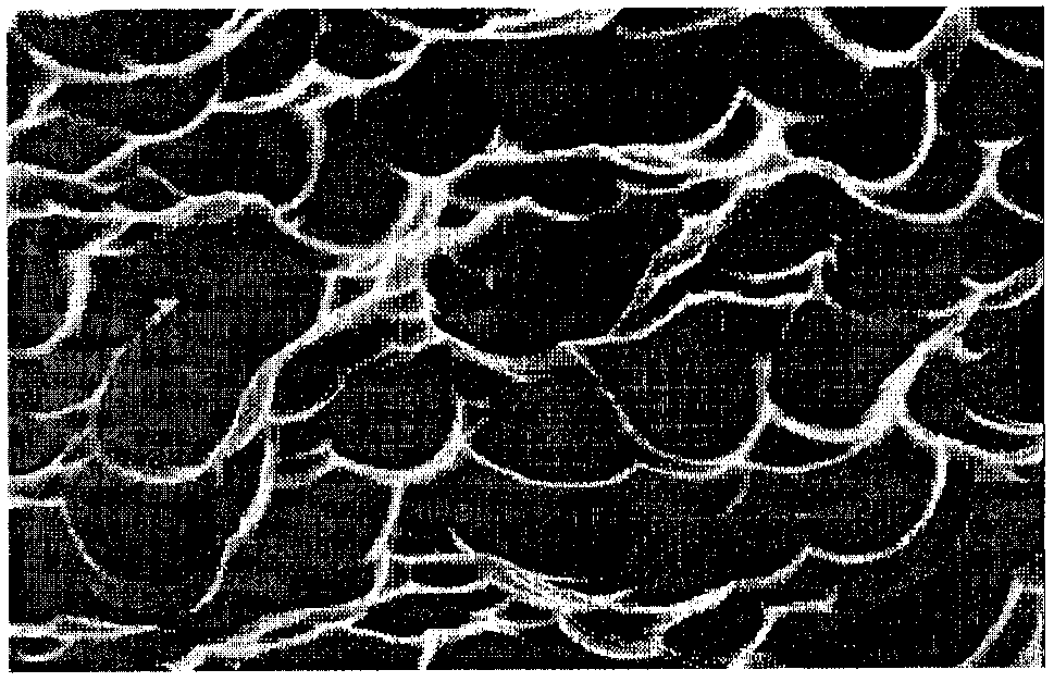
[0048] An isotropic texturing aqueous solution includes 10% hydrofluoric acid and 50% nitric acid. The pH of the acidic mixture texturing solution is less than 1. Use a conventional analytical balance to weigh 125mm 2 bulk doped polysilicon wafers and record their weights. The wafer was then immersed in the aqueous isotropic texturing solution at 10°C for 3 minutes. The wafer was then removed from the solution, rinsed with deionized water for 1 minute and dried at room temperature. Weigh the wafer. Based on the weight loss during texturing, the area of the wafer and the density of the silicon, the amount of etching on both sides of the wafer was calculated to be 4.5 μm using conventional methods. figure 1 5000X SEM of the surface of the textured wafer. There are no visible exposed grain boundaries.
[0049] Then utilize the MacBeth ColorEye TM A reflectometer measures the reflectivity of the wafer. Reflectance was recorded in 10 nm increments over the incident light ...
Embodiment 2
[0051] The following isotropic acidic aqueous texturing solutions were prepared.
[0052] Table 1
[0053] Element
Content-weight%
7.5%
1%
15%
water
margin
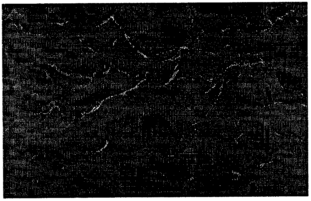
[0054] Weigh the bulk-doped polysilicon wafer and record its weight. It was then immersed in the solution at 80° C. for 10 minutes. The pH of the solution was 4. The wafer was then removed from the solution, rinsed with deionized water and air dried. The wafer was weighed and the amount of silicon etched from each side of the wafer was determined to be 4.73 μm. figure 2 Shown is the surface of the textured wafer. There are no visible exposed grain boundaries.
[0055] Then utilize the MacBeth ColorEye TM A reflectometer measures the reflectivity of the wafer. Reflectance was recorded in 10 nm increments over the wavelength range from 1100 nm down to 400 nm. The reflectomete...
PUM
| Property | Measurement | Unit |
|---|---|---|
| Thickness | aaaaa | aaaaa |
| Thickness | aaaaa | aaaaa |
Abstract
Description
Claims
Application Information