Semiconductor heterojunction solar cell based on bionic moth eye and manufacturing method thereof
A solar cell and semiconductor technology, applied in the field of solar cells, can solve the problems of ineffective utilization of incident light energy, the quality of the anti-reflection film depends on process conditions, and the increase of manufacturing costs, and achieves easy chip-level integration and mass production. , Conducive to the effect of efficiency and low cost
- Summary
- Abstract
- Description
- Claims
- Application Information
AI Technical Summary
Problems solved by technology
Method used
Image
Examples
Embodiment 1
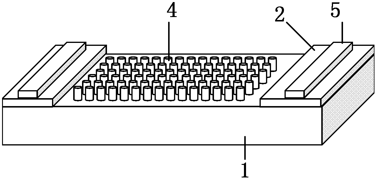
[0039] In this embodiment, when fabricating a bionic moth-eye heterojunction solar cell, firstly, SiO is thermally oxidized and grown on a single crystal semiconductor substrate 1, that is, an n-type silicon (100) substrate. 2 As the isolation layer 2, then sputter the metal electrode Ti / Pd / Au on the back of the single crystal semiconductor substrate 1 as the back electrode 3, then wet-etch the isolation layer 2 to form a window to expose the silicon surface, and use RIE to etch the silicon surface Form the silicon column array 4, the diameter of the silicon column is 200nm, the height is 200nm, and the pitch is 200nm. Finally, the metal front electrode 5 is prepared around the isolation layer window by the method of peeling off. The front electrode is a titanium (Ti) / gold (Au) stack layer, transfer the CVD-grown graphene directly onto the single crystal semiconductor substrate 1, make the graphene contact with the surface of the silicon pillar array 4 and the front electrode m...
Embodiment 2
[0041] In this embodiment, when fabricating a bionic moth-eye heterojunction solar cell, firstly, SiO is thermally oxidized and grown on a single crystal semiconductor substrate 1, that is, an n-type silicon (100) substrate. 2 As the isolation layer 2, then sputter the metal electrode Ti / Pd / Ag on the back of the silicon substrate as the back electrode 3, and then wet-etch the isolation layer 2 to form a window to expose the silicon surface, and use ICP to etch the silicon surface to form a silicon column Array 4. Finally, the ring-shaped metal front electrode 5 is prepared by peeling off. The front electrode is Ti / Au, and the semiconductor material 6 is prepared by thermal evaporation, that is, a copper iodide (CuI) film. CuI is filled between the silicon pillars to form a CuI / n-Si heterojunction solar cells.
Embodiment 3
[0043] The production of bionic moth-eye heterojunction solar cells in this example is similar to Example 2, the difference is that copper phthalocyanine (CuPc) is filled into the silicon column structure by vacuum deposition to form a CuPc / n-Si heterojunction Solar battery.
PUM
| Property | Measurement | Unit |
|---|---|---|
| diameter | aaaaa | aaaaa |
| diameter | aaaaa | aaaaa |
Abstract
Description
Claims
Application Information


