Heterojunction solar cell based on biomimetic moth-eye semiconductor and manufacturing method thereof

A technology of solar cells and semiconductors, applied in the field of solar cells, can solve the problems of ineffective use of incident light energy, the quality of anti-reflection coatings depends on process conditions, and increased manufacturing costs, etc., to achieve easy chip-level integration and mass production , Conducive to the effect of efficiency and low cost

Active Publication Date: 2011-11-30
TSINGHUA UNIV
View PDF6 Cites 16 Cited by
  • Summary
  • Abstract
  • Description
  • Claims
  • Application Information

AI Technical Summary

Problems solved by technology

Existing heterojunction solar cells usually adopt a planar structure, and the planar structure often cannot effectively use the incident light energy. For example, the reflectivity of planar silicon in the visible light range is as high as 30%, resulting in a large amount of energy loss.
At present, anti-reflection coatings such as silicon oxide and silicon nitride are widely used to reduce reflection. Anti-reflection coatings are based on the principle of light interference, and their thickness is 1 / 4 or 1 / 2 of the wavelength. Since a single-layer anti-reflection coating is only for a single wavelength It has a good anti-reflection effect, so if you need to have a good reflection effect on a wide range of light waves, you often need a multi-layer anti-reflection film, which will inevitably increase the manufacturing cost, and the quality of the anti-reflection film depends on the process conditions. Therefore, the effect of anti-reflection coating is limited

Method used


Image

  • Heterojunction solar cell based on biomimetic moth-eye semiconductor and manufacturing method thereof
  • Heterojunction solar cell based on biomimetic moth-eye semiconductor and manufacturing method thereof
  • Heterojunction solar cell based on biomimetic moth-eye semiconductor and manufacturing method thereof

Examples


Embodiment 1

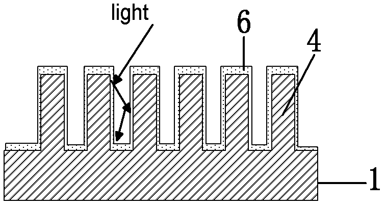
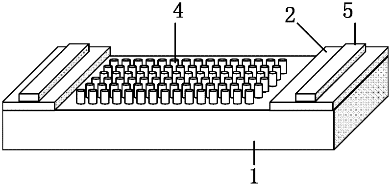
[0039] In this embodiment, when fabricating a bionic moth-eye heterojunction solar cell, firstly, SiO is thermally oxidized and grown on a single crystal semiconductor substrate 1, that is, an n-type silicon (100) substrate. 2 As the isolation layer 2, then sputter the metal electrode Ti / Pd / Au on the back of the single crystal semiconductor substrate 1 as the back electrode 3, then wet-etch the isolation layer 2 to form a window to expose the silicon surface, and use RIE to etch the silicon surface Form the silicon column array 4, the diameter of the silicon column is 200nm, the height is 200nm, and the pitch is 200nm. Finally, the metal front electrode 5 is prepared around the isolation layer window by the method of peeling off. The front electrode is a titanium (Ti) / gold (Au) stack layer, transfer the CVD-grown graphene directly onto the single crystal semiconductor substrate 1, make the graphene contact with the surface of the silicon pillar array 4 and the front electrode m...

Embodiment 2

[0041] In this embodiment, when fabricating a bionic moth-eye heterojunction solar cell, firstly, SiO is thermally oxidized and grown on a single crystal semiconductor substrate 1, that is, an n-type silicon (100) substrate. 2 As the isolation layer 2, then sputter the metal electrode Ti / Pd / Ag on the back of the silicon substrate as the back electrode 3, and then wet-etch the isolation layer 2 to form a window to expose the silicon surface, and use ICP to etch the silicon surface to form a silicon column Array 4. Finally, the ring-shaped metal front electrode 5 is prepared by peeling off. The front electrode is Ti / Au, and the semiconductor material 6 is prepared by thermal evaporation, that is, a copper iodide (CuI) film. CuI is filled between the silicon pillars to form a CuI / n-Si heterojunction solar cells.

Embodiment 3

[0043] The production of bionic moth-eye heterojunction solar cells in this example is similar to Example 2, the difference is that copper phthalocyanine (CuPc) is filled into the silicon column structure by vacuum deposition to form a CuPc / n-Si heterojunction Solar battery.


PUM

PropertyMeasurementUnit
diameteraaaaaaaaaa
diameteraaaaaaaaaa

Abstract

The invention relates to a semiconductor heterojunction solar cell based on a bionic moth eye and a manufacturing method thereof. The manufacturing method comprises the following steps: depositing silicon oxide (SiO2) or silicon nitride (Si3N4) on a single crystal semiconductor substrate to obtain an isolating layer; preparing a bionic moth eye array on the surface of the single crystal semiconductor substrate; evaporating metal on the back side of the substrate, thereby forming a back electrode; preparing a metal front electrode on the surface of the isolating layer; and filling a semiconductor material in the array to form the heterojunction. The manufactured semiconductor heterojunction solar cell has the advantages that the structure is simple, the manufacturing process is easy, the reflection of incident light is efficiently reduced and the contact area of the heterojunction is increased, thereby achieving the purpose of promoting the energy conversion efficiency of the solar cell.

Description

technical field [0001] The invention belongs to the technical field of solar cells, in particular to a bionic moth-eye semiconductor heterojunction solar cell and a manufacturing method thereof. Background technique [0002] The semiconductor heterojunction solar cell is an important structure in the existing solar cells. It is composed of two semiconductor materials with different energy band structures. The energy bands on the contact surface are bent or mutated to form a built-in electric field, thereby providing light for light generation. The voltaic effect provides the conditions for the separation of carriers generated in semiconductors. Due to the diversity of semiconductor materials, the choice of materials constituting heterojunction solar cells is also very flexible. At present, amorphous silicon / single crystal silicon heterojunction, InGaP / GaAs heterojunction, CdS / CdTe heterojunction, and organic heterojunction are the most used in semiconductor heterojunction s...

Claims


Application Information

Patent Timeline
Patent Type & Authority Applications(China)
IPC IPC(8): H01L31/0352H01L31/072H01L31/18H01L51/42
CPCY02E10/549Y02E10/50Y02P70/50
Inventor 谢丹冯婷婷任天令宋睿田禾李虓吴德海朱宏伟
Owner TSINGHUA UNIV
Why Eureka
Try Eureka