Manufacture method of Schottky photovoltaic cell based on graphene and silicon reverse pyramid array

An inverted pyramid, photovoltaic cell technology, applied in the field of solar cells, can solve the problems of light energy loss, inability to effectively utilize incident light energy, etc., and achieve the effects of reducing preparation costs, improving photoelectric conversion efficiency, and small reflection coefficient

Inactive Publication Date: 2017-08-29
YUNNAN UNIV
View PDF8 Cites 7 Cited by
  • Summary
  • Abstract
  • Description
  • Claims
  • Application Information

AI Technical Summary

Problems solved by technology

Although the photoelectric conversion efficiency is low, its simple structure, easy preparation, low cost, and environmental protection make it have great potential for development in photovoltaic cells.
In the literature, the graphene-silicon Schottky junction adopts a planar structure, and the planar structure often cannot effectively use the incident light energy. For example, the reflectivity of planar silicon in the visible light range is as high as 30%, resulting in a large loss of light energy.

Method used


Image

  • Manufacture method of Schottky photovoltaic cell based on graphene and silicon reverse pyramid array
  • Manufacture method of Schottky photovoltaic cell based on graphene and silicon reverse pyramid array
  • Manufacture method of Schottky photovoltaic cell based on graphene and silicon reverse pyramid array

Examples


Embodiment 1

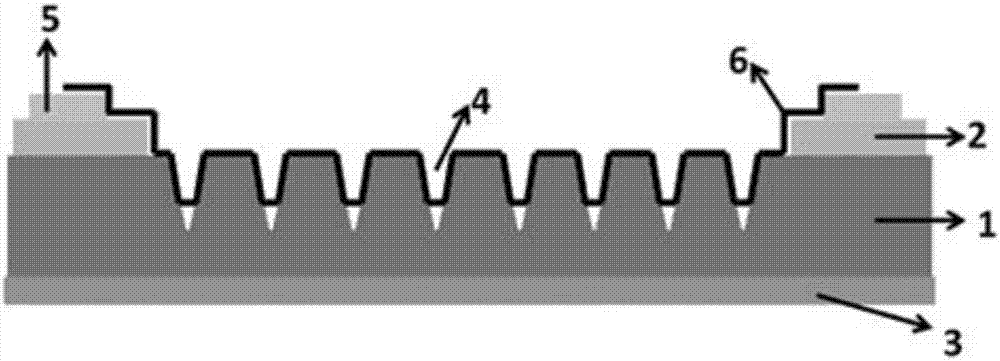
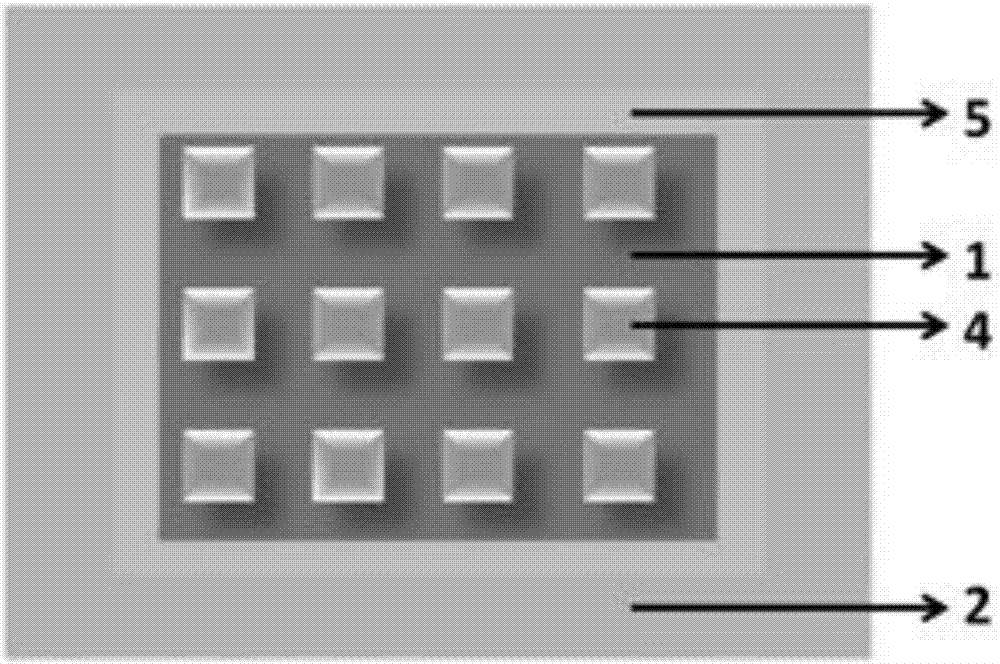
[0032] In this embodiment, when fabricating a graphene-silicon inverted pyramid array Schottky junction photovoltaic cell, first thermally oxidize a single crystal silicon substrate 1 with an n-type (100) resistivity of 1-10 Ω cm, and thermally oxidize and grow SiO with a thickness of 300 nm. 2 as SiO 2 For the isolation layer 2, the oxide layer on the back of the silicon substrate 1 is removed by wet etching, and then the metal In / Ga alloy is applied on the back of the single crystal silicon substrate 1 as the back electrode 3, and SiO is wet etched. 2 The isolation layer 2 forms a window to expose the original silicon surface. The silicon surface is etched by MACE to form a silicon inverted pyramid array 4. The etching time is 15 minutes. The depth of the silicon inverted pyramid hole is about 2 microns, and the diameter is 1 micron. The method of electron beam evaporation prepares the metal front electrode 5 around the isolation layer window, the metal material is Au, and t...

Embodiment 2

[0034] This example makes a graphene silicon inverted pyramid array Schottky photovoltaic cell, similar to Example 1, the difference is that cyclododecane is used to transfer graphene, the process of transferring graphene is simpler, the surface is cleaner, and the prepared device The photoelectric conversion efficiency is 3.50%.

Embodiment 3

[0036] This example makes a graphene silicon inverted pyramid array Schottky photovoltaic cell, similar to Example 1, the difference is that the graphene transparent electrode is p-doped with nitric acid to improve the work function and conductivity of graphene, and then transfer and prepare The photoelectric conversion efficiency of the prepared device is 5.63%.


PUM

PropertyMeasurementUnit
electrical resistivityaaaaaaaaaa
thicknessaaaaaaaaaa
crystal orientationaaaaaaaaaa

Abstract

The invention relates to a manufacture method of a Schottky photovoltaic cell based on graphene and a silicon reverse pyramid array. Silicon oxide (SiO2) is grown on a monocrystalline n-Si semiconductor substrate by thermooxidizing and serves as an isolation layer, hydrofluoric acid (HF) is used to corrode the SiO2 isolation layer to form a window, the SiO2 isolation layer in the periphery of the window and the back side of a semiconductor are coated with an insulating tape and thus protected, the silicon reverse pyramid array is prepared in the window by using a metal-assisted chemical etching method, the insulating tape is torn, cleaning is carried out, the back side of the substrate is smeared with In/Ga alloy to serve as a back electrode, metal Au is evaporated and deposited on the isolation layer to serve as a front electrode, and graphene is transferred onto the silicon reverse pyramid array and is electrically connected with the front electrode. The photovoltaic cell is simple in structure, easy to prepare and low in cost, reflection of incident light is reduced effectively, the Schottky junction contact area is increased, and the conversion efficiency of the photovoltaic cell is improved.

Description

technical field [0001] The invention belongs to the technical field of solar cells, and relates to a method for preparing a graphene-silicon inverted pyramid array Schottky junction photovoltaic cell. Background technique [0002] With the increasing global environmental pollution and the increasingly tense energy situation, energy issues have gradually attracted the attention of countries all over the world. At present, energy is mainly composed of traditional fossil fuels such as oil and coal, but these energy sources are non-renewable energy sources, and their dwindling storage capacity is difficult to meet the growing demand of human beings. For sustainable development, renewable energy sources are becoming more and more popular. human concern. Among them, the energy of solar energy is huge, inexhaustible, widely distributed, suitable for use in most parts of the world, the materials used are safe and reliable, and there is no environmental pollution, so it has great pr...

Claims


Application Information

Patent Timeline
Patent Type & Authority Applications(China)
IPC IPC(8): H01L31/07H01L31/0236H01L31/0224H01L31/18
CPCH01L31/022425H01L31/022466H01L31/02363H01L31/07H01L31/1804Y02E10/547Y02P70/50
Inventor 陈秀华尚钰东马文会
Owner YUNNAN UNIV
Why Eureka
Try Eureka