Surface conduction electron emission source based on oxide nanostructure and its manufacturing method

A nano-structured, electron-conducting technology, applied in electrode system manufacturing, discharge tube/lamp manufacturing, cathode ray tube/electron beam tube, etc., can solve the problems of complex manufacturing process, low emission efficiency, low electron emission efficiency, etc.

Active Publication Date: 2011-11-30
FUZHOU UNIV
View PDF4 Cites 9 Cited by
  • Summary
  • Abstract
  • Description
  • Claims
  • Application Information

AI Technical Summary

Problems solved by technology

[0006] (2) Low electron emission efficiency: Since the electron emission gap is only a few nanometers in width, many electrons have been collected by the grid before being extracted by the anode electric field. lead to low emission efficiency
However, if the gap is increased, a higher voltage is required to emit electrons, which will increase the complexity of the driving circuit
[0007](3) The manufacturing process is complicated, and the electron emission layer is limited to a discontinuous metal oxide film

Method used


Image

  • Surface conduction electron emission source based on oxide nanostructure and its manufacturing method
  • Surface conduction electron emission source based on oxide nanostructure and its manufacturing method
  • Surface conduction electron emission source based on oxide nanostructure and its manufacturing method

Examples


preparation example Construction

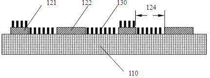
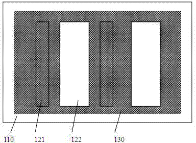
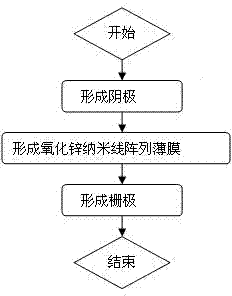
[0058] A method for preparing a surface conduction electron emission source based on zinc oxide nanowires provided in the first embodiment of the present invention includes the following steps:

[0059] Step 1, refer to Figure 4 , form the cathode electrode 121 on the surface of the substrate 110, and the material used for the cathode electrode 121 can be photosensitive silver paste, Cu, W, Co, Ni, Ta, TaN, Ti, Zn, Al, or other metal electrodes. The present embodiment preferably adopts photosensitive silver paste, and its specific process includes:

[0060] (a) Spin coating of photosensitive silver paste: the photosensitive silver was transferred to the surface of the substrate 110 by using a spin coating process, and kept at 110° C. for 20 minutes. The substrate used can be selected from glass, quartz, ceramics, and high temperature resistant materials with an insulating layer on the surface;

[0061] (b) Exposure: The pre-dried photosensitive silver paste film layer is na...


PUM


Abstract

The invention discloses an oxide-nano-structure-based surface-conduction electron emission source and a manufacturing method thereof. The surface-conduction electron emission source comprises a glass substrate, cathodes and grids which are positioned on the surface of the glass substrate in parallel in a staggered way, and electron emission layers which are arranged on the surfaces of the cathodes and in gaps between the cathodes and the grids and have an oxide nano structure. In the oxide-nano-structure-based surface-conduction electron emission source, the high electron emission performanceof the electron emission layer having a planar field emission structure and the high electron emission performance of the electron emission layer having the oxide nano structure are combined effectively; the electron emission layers having the oxide nano structures form an oxide nano structure array; and the array is positioned on the surfaces of the cathodes and in the gaps between the cathodes and the grids. The electron emission layers having the oxide nano structures in the array can be used as an electron emission source and a surface electron conduction layer, and the electron emission current density is large and the electron emission efficiency is high; furthermore, the process is simple, the cost is low and the emission is stable and reliable.

Description

technical field [0001] The invention relates to a surface conduction electron emission flat panel display technology, in particular to an electron emission source of a surface conduction electron emission flat panel display and a manufacturing method thereof. Background technique [0002] Surface-conduction Electron-emitter Display (SED) is a planar field emission cathode structure. As a display with superior performance, its manufacturing process does not require high-cost and high-precision semiconductor technology. It is produced under ordinary conditions; and the surface conduction emitter it has is a planar field emission structure, and the emission performance is much more stable. The history of the surface conduction electron emission phenomenon can be traced back to the early 1960s, when it was discovered by former Soviet scholars, and it was generally classified as thin film field emission. The key part of SED is the manufacture of the lower substrate, that is, the...

Claims


Application Information

Patent Timeline
Patent Type & Authority Applications(China)
IPC IPC(8): H01J29/04H01J9/02
Inventor 张永爱郭太良叶芸胡利勤吴朝兴郑泳
Owner FUZHOU UNIV
Why Eureka
Try Eureka