A kind of multi-junction tandem solar cell and its manufacturing method

A solar cell and manufacturing method technology, applied in circuits, photovoltaic power generation, electrical components, etc., can solve the problems of low quality of battery materials, affect efficiency, lattice mismatch, etc., to solve lattice mismatch and improve utilization efficiency. , the effect of improving battery efficiency

Inactive Publication Date: 2011-12-07
SUZHOU INST OF NANO TECH & NANO BIONICS CHINESE ACEDEMY OF SCI
View PDF4 Cites 16 Cited by
  • Summary
  • Abstract
  • Description
  • Claims
  • Application Information

AI Technical Summary

Problems solved by technology

However, the problem brought about by this is that too many material systems are used on the same substrate, resulting in seri

Method used


Image

  • A kind of multi-junction tandem solar cell and its manufacturing method
  • A kind of multi-junction tandem solar cell and its manufacturing method
  • A kind of multi-junction tandem solar cell and its manufacturing method

Examples


Embodiment 1

[0045] The manufacturing method of the multi-junction laminated solar cell provided in this embodiment includes the following steps:

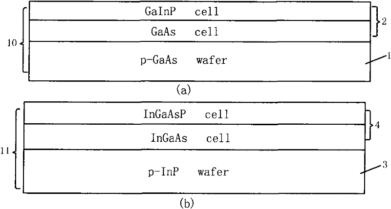
[0046] 1. Use molecular beam epitaxy (MBE) or metal organic chemical vapor deposition (MOCVD) methods to sequentially grow GaAs and GaInP epitaxial layers 2 on p-GaAs substrate 1 to obtain upper battery cell 10, see figure 1 (a); InGaAs, InGaAsP epitaxial layer 4 is grown sequentially on p-InP substrate 3 to obtain bottom battery cell 11, see figure 1 (b). The above two battery cells are double junction battery cells, and the lattice of each battery cell is completely matched.

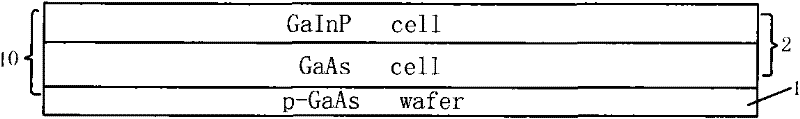
[0047] 2. Use chemical mechanical polishing (CMP) method to thin and polish the substrate 1 in the upper battery cell 10 to below 150μm, see figure 2 , In order to reduce the part of incident light that is absorbed in the transmission process.

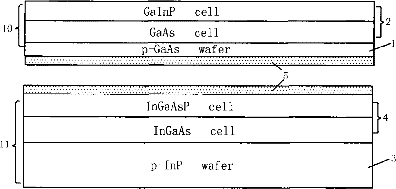
[0048] 3. A metal thin film layer 5 is vapor-deposited on the back of the substrate 1 of the upper battery cell 10 and on the top of...

Embodiment 2

[0053] The manufacturing method of the multi-junction laminated solar cell provided in this embodiment includes the following steps:

[0054] 1. Use molecular beam epitaxy (MBE) or metal organic chemical vapor deposition (MOCVD) method to grow GaAs, GaInP epitaxial layer 2 on p-GaAs substrate 1 in order to obtain upper battery cell 10, see figure 1 (a); InGaAs, InGaAsP epitaxial layer 4 is sequentially grown on p-InP substrate 2 to obtain bottom battery cell 11, see figure 1 (b). The above two battery cells are both double-junction battery cells, and the lattice of each battery cell is completely matched.

[0055] 2. Use chemical mechanical polishing (CMP) method to thin and polish the substrate 1 in the upper battery cell 10 to below 150μm, see figure 2 In order to reduce the part of the incident light that is absorbed in the transmission process.

[0056] 3. A layer of antireflection and antireflection film 6 is vapor-deposited on the back of the substrate 1 of the upper battery c...

Embodiment 3

[0061] The manufacturing method of the multi-junction laminated solar cell provided in this embodiment includes the following steps:

[0062] 1. Use molecular beam epitaxy (MBE) or metal organic chemical vapor deposition (MOCVD) methods to sequentially grow InGaAs and InGaAsP epitaxial layers 4 on p-InP substrate 3 to obtain bottom cell 11, see Picture 9 (b).

[0063] On the p-GaAs substrate 1, molecular beam epitaxy (MBE) or metal organic chemical vapor deposition (MOCVD) is used to grow a layer of corrosion barrier layer 9 with a thickness of 50-1000 nm. The material of the corrosion barrier layer 9 is AlGaAs, and then using the same method to grow GaInP and GaAs materials on the corrosion barrier layer 9 to form the epitaxial layer 2 to obtain the upper battery cell 10, see Picture 9 (a). It is worth noting that the material layers of this upper battery cell 10 from bottom to top are p-GaAs, AlGaAs, GaInP, and GaAs respectively. Compared with the epitaxial layer 2 of the upper...


PUM

PropertyMeasurementUnit
Thicknessaaaaaaaaaa

Abstract

The invention relates to a multijunction laminated solar cell and a manufacturing method thereof. The multijunction laminated solar cell comprises a cell unit laminated body (A) as well as a top electrode (12) and a back electrode (13) which are arranged on the top and bottom of the cell unit laminated body (A), wherein the cell unit laminated body (A) comprises a bottom-layer cell unit (11) and at least one upper-layer cell unit (10) connected to the top of the bottom-layer cell unit (11) in a laminating manner; the bottom-layer cell unit (11) comprises a substrate (3) and an epitaxial layer(4); the upper-layer cell unit (10) at least comprises an epitaxial layer (2); and the cell unit laminated body (A) can be obtained by performing direct bonding, metallic bonding or inversed welding processes on the bottom-layer cell unit (11) and the upper-layer cell unit (10). According to the invention, not only can the problem of unmatched crystal lattice of the cell unit laminated body (A) is solved, but also the overall working efficiency of the solar cell is improved.

Description

Technical field [0001] The invention belongs to the field of solar cell manufacturing and application, in particular to a laminated solar cell and a manufacturing method thereof. Background technique [0002] The existing mass-produced solar cells are mainly made of materials such as silicon and GaAs. The efficiency of a single junction cell using a single material is generally not very high. The usual way is to grow multiple materials such as GaInP, InGaAs, and Ge on the same substrate, and then make solar cells. However, the problem brought about by this is that too many material systems are used on the same substrate, resulting in serious lattice mismatch, resulting in low-quality battery materials and affecting efficiency. It is of practical significance to develop a solar cell that can realize multi-junction series connection and is not affected by the limitation of the crystal lattice. Summary of the invention [0003] The invention provides a multi-junction laminated sol...

Claims


Application Information

Patent Timeline
IPC IPC(8): H01L31/078H01L31/0216H01L31/0224H01L31/18
CPCY02E10/50Y02P70/50
Inventor 何巍黄寓洋陆书龙董建荣杨辉
Owner SUZHOU INST OF NANO TECH & NANO BIONICS CHINESE ACEDEMY OF SCI
Why Eureka
Try Eureka