Method for making selective emitter crystalline silicon solar cell

A solar cell and crystalline silicon technology, applied in circuits, electrical components, semiconductor devices, etc., can solve the problems of low battery efficiency, inability to apply, and reduced overall battery performance, avoiding multiple high-temperature damage and high battery conversion efficiency. , the effect of avoiding equipment costs

Active Publication Date: 2012-12-19
NINGBO ULICA SOLAR SCIENCE & TECHNOLOGY CO LTD
View PDF3 Cites 0 Cited by
  • Summary
  • Abstract
  • Description
  • Claims
  • Application Information

AI Technical Summary

Problems solved by technology

However, there are problems at the same time that the surface doping concentration of the shallow junction cell is low, the ohmic contact between the front grid electrode and the cell is deteriorated, and the contact resistance is increased, resulting in a decrease in the fill factor of the crystalline silicon solar cell and a decrease in the overall performance of the cell.
Because the phosphorus concentration obtained by volatile deposition is not as high as that in the electrode area, heavy diffusion is formed in the electrode area, and light diffusion is formed in the non-electrode area to obtain a selective emitter structure. However, the PN junction obtained by this diffusion method is very uneven. The diffusion concentration is high near the phosphorous slurry, and the concentration is low far away, so the battery efficiency is not high
[0009] In addition, there are photolithography, laser slotting and other technologies to produce selective emitter crystalline silicon solar cells, but these production methods have problems such as high cost and complicated process, which do not meet the dual requirements of preparing high-efficiency and low-cost crystalline silicon solar cells. Requirements, poor repeatability, cannot be applied in industrial mass production

Method used


Image

  • Method for making selective emitter crystalline silicon solar cell

Examples


Embodiment 1

[0024] A method for preparing a selective emitter P-type monocrystalline silicon solar cell, comprising the following steps:

[0025] ① Make the P-type monocrystalline silicon wafer suede, then wash and dry it. Suede making and cleaning adopt prior art.

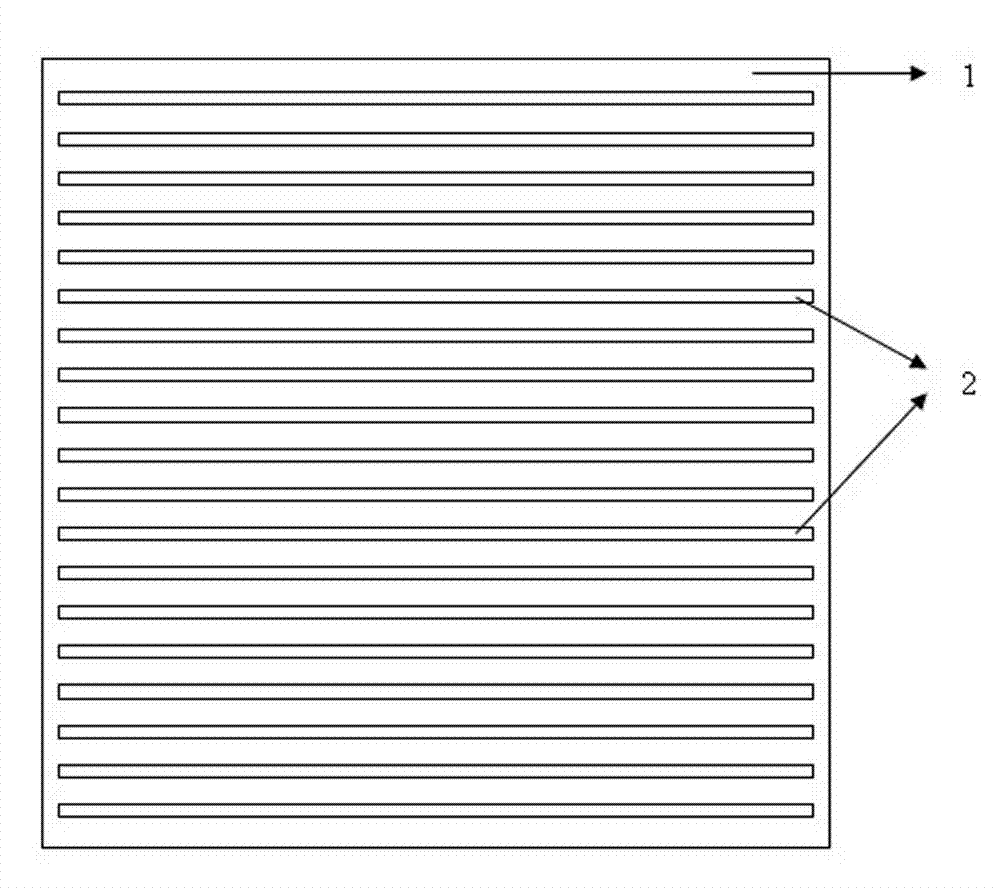
[0026] ②Put the P-type single crystal silicon wafer obtained in step ① on the loading table of the linear magnetron sputtering coating machine, cover the mask plate 1, fix the silicon wafer and the mask plate 1, and then put it into the magnetron sputtering coating machine. In the magnetron sputtering chamber of the sputtering coating machine, the antimony pre-fixed in the magnetron sputtering chamber is used as the target for sputtering. Close the door of the magnetron sputtering chamber, evacuate the magnetron sputtering chamber, set the sputtering pressure to 0.7Pa, the argon flow rate to 15sccm, the substrate temperature to 240°C, and the sputtering time to 25s. The mask plate is removed to realize the antimony film dep...

Embodiment 2

[0030] A method for preparing a selective emitter P-type polycrystalline silicon solar cell, comprising the following steps:

[0031] ① Make the P-type polysilicon wafer suede, then wash and dry it. Suede making and cleaning adopt prior art.

[0032]② Put the P-type polysilicon wafer obtained in step ① on the loading table of the linear magnetron sputtering coating machine, cover the mask plate 1, fix the silicon wafer and the mask plate 1, and then put it into the magnetron sputtering coating machine In the magnetron sputtering chamber of the machine, the antimony pre-fixed in the magnetron sputtering chamber is used as the target for sputtering. Close the door of the magnetron sputtering chamber, evacuate the magnetron sputtering chamber, set the sputtering pressure to 0.9Pa, the argon flow rate to 18sccm, the substrate temperature to 240°C, and the sputtering time to 30s. The mask plate is removed, and the antimony film deposition on the positive electrode gate line regio...


PUM

PropertyMeasurementUnit
widthaaaaaaaaaa

Abstract

The invention discloses a method for making a selective emitter crystalline silicon solar cell. The method comprises the following steps of: making a texture surface of a crystalline silicon wafer, cleaning and drying; coating a mask plate (1) on the surface and fixing; placing into a magnetron sputtering chamber of a magnetron sputtering coating machine; sputtering by taking antimony as a target; removing the mask plate (1) after sputtering is finished; placing into a diffusion furnace pipe to diffuse a liquid phosphorus source; and etching, removing phosphorosilicate glass, plating a silicon nitride film, printing and sintering to obtain the selective emitter crystalline silicone solar cell. The method is high in repeatability, low in cost and applicable to industrialized mass production. Moreover, the selective emitter crystalline solar cell prepared by the method is high in conversion efficiency.

Description

technical field [0001] The invention relates to the field of preparation of crystalline silicon solar cells, in particular to a method for preparing a selective emitter crystalline silicon solar cell. Background technique [0002] At present, the preparation methods of conventional crystalline silicon solar cells are as follows: remove the damaged layer of the silicon wafer and form a textured structure; chemically clean and dry; diffuse the liquid phosphorus source to form a uniformly doped PN junction; remove the peripheral PN junction and surface formed during the diffusion process. Phospho-silicate glass; anti-reflection film deposited on the surface; making the back electrode, back electric field and front electrode of the battery; co-sintering makes the electrode and the battery form a good ohmic contact, and completes the entire battery preparation process. [0003] The development direction of crystalline silicon solar cells is low cost and high efficiency. At prese...

Claims


Application Information

Patent Timeline
Patent Type & Authority Patents(China)
IPC IPC(8): H01L31/18
CPCY02P70/50
Inventor 刘伟万青陈筑刘晓巍徐晓群
Owner NINGBO ULICA SOLAR SCIENCE & TECHNOLOGY CO LTD
Why Eureka
Try Eureka