Gan-based light-emitting diode chip and manufacturing method thereof
A technology of LED chips and electrodes, applied in electrical components, circuits, semiconductor devices, etc., can solve the problems of high equipment cost and low yield, and achieve the effect of reducing production costs
- Summary
- Abstract
- Description
- Claims
- Application Information
AI Technical Summary
Problems solved by technology
Method used
Image

Examples
Embodiment approach 1
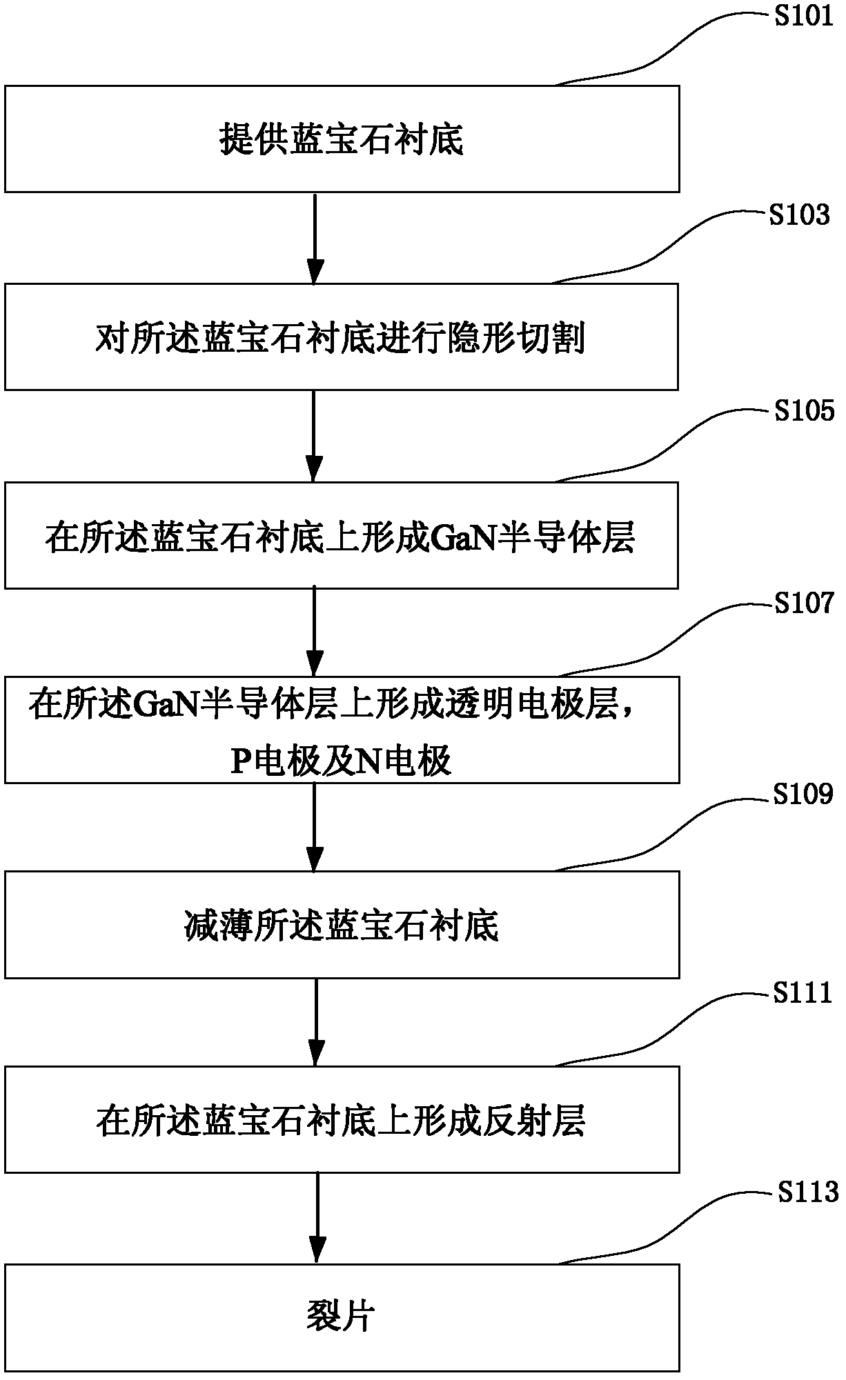
[0030] Such as figure 1 As shown, the preparation method of the GaN-based LED chip of the present invention comprises the following steps:
[0031] S101: providing a sapphire substrate;
[0032] S103: Stealth cutting the sapphire substrate;
[0033] S105: forming a GaN semiconductor layer on the sapphire substrate;
[0034] S107: forming a transparent conductive layer, a P electrode and an N electrode on the GaN semiconductor layer;
[0035] S109: Thinning the sapphire substrate;
[0036] S111: forming a reflective layer on the sapphire substrate; and
[0037] S113: Splinter.
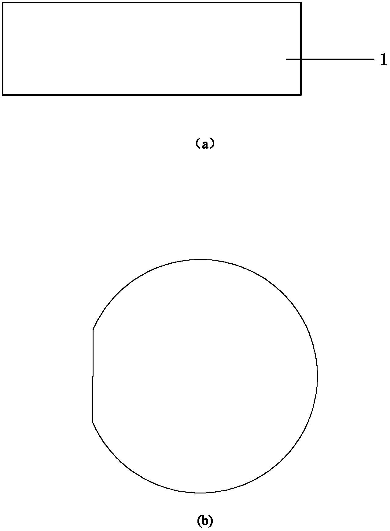
[0038] The following combination Figure 1 to Figure 10 The method of manufacturing the GaN-based LED chip according to Embodiment 1 of the present invention will be described in detail. Specifically, step S101 is firstly performed, that is, providing a sapphire substrate. The substrate used in this embodiment is a flat sapphire substrate 101, the front view of which is as figure 2 As shown in (...
Embodiment approach 2
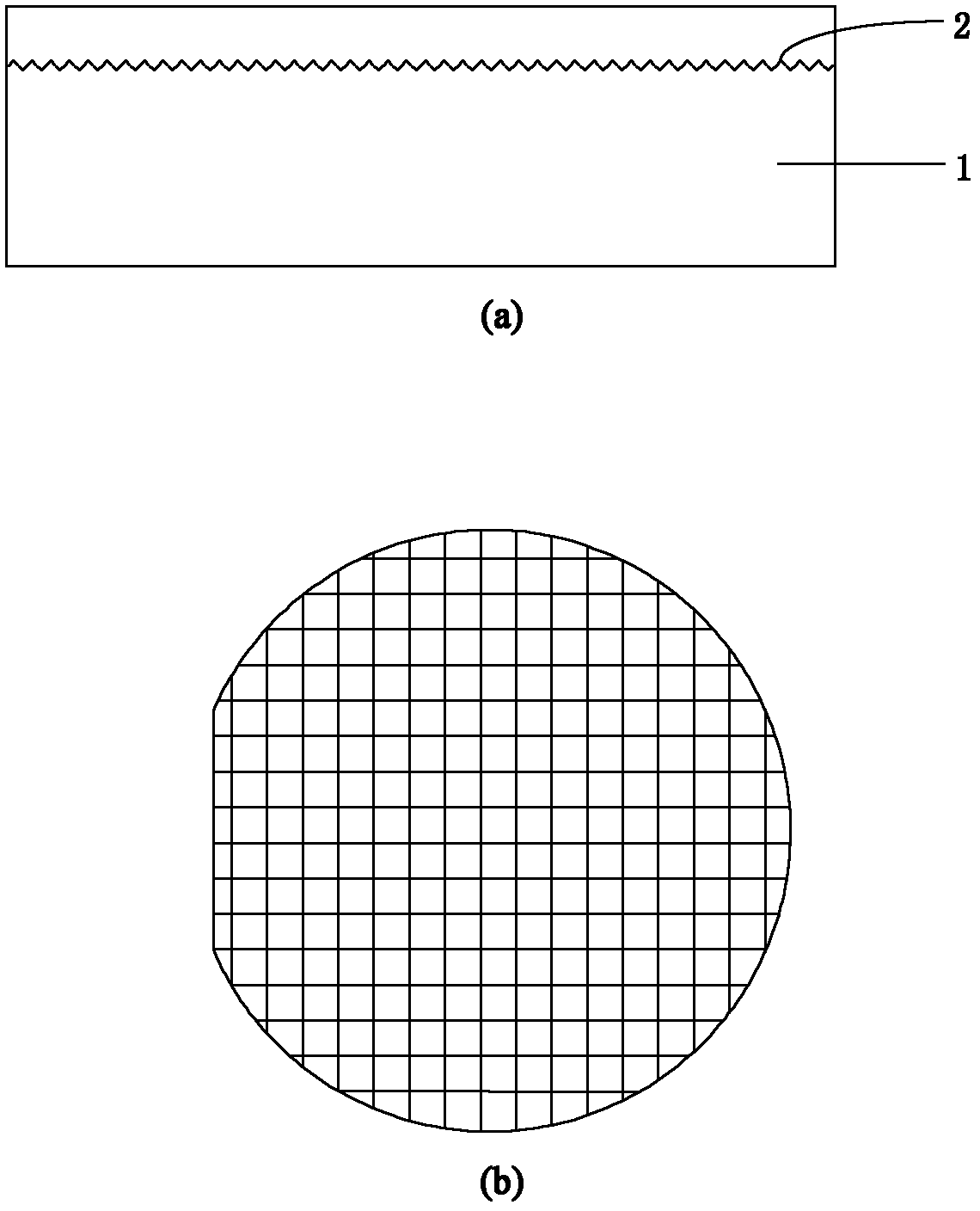
[0047] Embodiment 2 differs from Embodiment 1 in that the flat sapphire substrate 101 in Embodiment 1 is replaced by a patterned sapphire substrate PSS 201 . The front view of PSS 201 is as Figure 11 shown. The structure after vapor deposition of reflective layer 210 on the back of PSS 201 by vapor deposition technology is as follows Figure 12 As shown, it includes an N-type GaN layer 203, a quantum well layer 204, a P-type GaN layer 205, an N electrode 207, a P electrode 208, a protective film layer 209 and a reflective layer 210, and its preparation method, mutual positional relationship and structure are respectively related to The corresponding components in Embodiment 1 are the same, so the related description is omitted here. In addition, in Figure 12 In , the invisible cutting line is marked by reference numeral 12 .
Embodiment approach 3
[0049] In Embodiments 1 and 2, when performing step S107, that is, when forming the above-mentioned transparent conductive layer, the above-mentioned N electrode, and the above-mentioned P electrode on the above-mentioned GaN semiconductor layer, the transparent conductive layer is first formed on the above-mentioned GaN semiconductor layer, and then Using photolithography and etching technology to partially etch the above-mentioned transparent conductive layer and GaN semiconductor layer, so that the above-mentioned N-type GaN layer is partially exposed, such as Figure 5 and 6 shown.
[0050] The difference from Embodiments 1 and 2 is that in this embodiment, in the step S107 of forming the above-mentioned transparent conductive layer, the above-mentioned N electrode and the above-mentioned P electrode, the above-mentioned GaN semiconductor layer is first partially processed by photolithography and etching technology. Etching to partially expose the above-mentioned N-type G...
PUM
| Property | Measurement | Unit |
|---|---|---|
| Thickness | aaaaa | aaaaa |
| Wavelength | aaaaa | aaaaa |
Abstract
Description
Claims
Application Information