A kind of vertical structure light-emitting diode and its manufacturing method

A light-emitting diode and vertical structure technology, which is applied in the direction of electrical components, circuits, semiconductor devices, etc., can solve the problems of complex process, improvement, and unfavorable yield rate, etc., and achieve the effect of increasing light output area, reducing film stress, and reducing debris phenomenon

Active Publication Date: 2011-12-28
EPILIGHT TECH
View PDF5 Cites 9 Cited by
  • Summary
  • Abstract
  • Description
  • Claims
  • Application Information

AI Technical Summary

Problems solved by technology

However, the process of peeling off the sapphire substrate is often complicated, which is not conducive to the improvement of the yield rate in production

Method used


Image

  • A kind of vertical structure light-emitting diode and its manufacturing method
  • A kind of vertical structure light-emitting diode and its manufacturing method
  • A kind of vertical structure light-emitting diode and its manufacturing method

Examples


Embodiment Construction

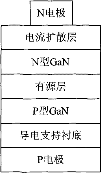
[0025] Please see Figure 2 to Figure 7 , specifically illustrate the implementation process of the vertical structure light-emitting diode manufacturing method of the present invention:

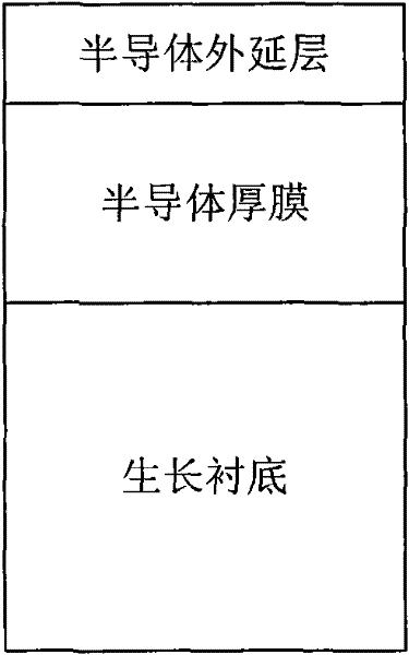
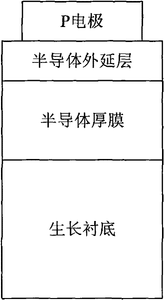
[0026] Step 1, growing a semiconductor thick film on the growth substrate, and then growing a semiconductor epitaxial layer on the semiconductor thick film, the semiconductor epitaxial layer at least includes an N-type semiconductor layer, an organic layer located on the N-type semiconductor layer source layer, and a P-type semiconductor layer located on the active layer, such as figure 2 shown.

[0027] Among them, chemical vapor deposition (CVD), plasma chemical vapor deposition (PECVD), metal compound vapor deposition (MOCVD), molecular beam epitaxy (MBE) and other methods can be used to grow semiconductor thick films and semiconductor epitaxial layers. The growth substrate is a Si substrate, a SiC substrate or a sapphire substrate, and a sapphire substrate is preferred in this embodim...


PUM


Abstract

The invention discloses an LED (light emitting diode) with a vertical structure and a manufacturing method thereof. The LED structure comprises an N electrode, a semiconductor thick film arranged on the N electrode, a semiconductor epitaxial layer arranged on the semiconductor thick film and a P electrode arranged on the semiconductor epitaxial layer. The structure uses a P-type semiconductor layer as a light emitting surface, the light-emitting area can be increased and the light-emitting efficiency can be improved compared with that of an electrode structure at the same side. The manufacturing method of the LED with the vertical structure utilizes a temporary bonding process and a thick film process and uses a temporary substrate to support grinding and remove the growing substrate; compared with the usual vertical structure process, a laser lift-off process can be used to reduce the damage to GaN and the fragment phenomenon caused by the problems such as bonding process unevenness and the like, thus the rate of qualified products of the chip with the vertical structure can be improved.

Description

technical field [0001] The invention relates to a structure of a light emitting diode and a manufacturing method thereof, in particular to a light emitting diode with a vertical structure and a manufacturing method thereof. Background technique [0002] Light-emitting diodes have the advantages of small size, high efficiency and long life, and are widely used in traffic indication, outdoor full-color display and other fields. In particular, the use of high-power light-emitting diodes may realize semiconductor solid-state lighting, which has caused a revolution in the history of human lighting, and has gradually become a research hotspot in the field of electronics. The light extraction efficiency of LED refers to the ratio of the available photons incident to the device and the photons generated by electron-hole recombination in the active area of ​​the epitaxial wafer. In traditional LED devices, due to factors such as substrate absorption, electrode blocking, and total re...

Claims


Application Information

Patent Timeline
Patent Type & Authority Applications(China)
IPC IPC(8): H01L33/36
Inventor 张楠朱广敏叶青潘尧波齐胜利郝茂盛
Owner EPILIGHT TECH
Why Eureka
Try Eureka