Three-dimensional storage device array structure and manufacturing method thereof

A technology of a memory array and a manufacturing method, which is applied in the field of a three-dimensional memory array structure and its manufacturing, can solve the problems of high process temperature, unsatisfactory forward current density, and difficulty in metal electrode manufacturing.

Active Publication Date: 2012-01-04
XIAMEN IND TECH RES INST CO LTD
View PDF3 Cites 14 Cited by
  • Summary
  • Abstract
  • Description
  • Claims
  • Application Information

AI Technical Summary

Problems solved by technology

Diodes based on single crystal Si materials have high current density and rectification ratio, but the process temperature is high, and it is n

Method used


Image

  • Three-dimensional storage device array structure and manufacturing method thereof
  • Three-dimensional storage device array structure and manufacturing method thereof
  • Three-dimensional storage device array structure and manufacturing method thereof

Examples


Embodiment Construction

[0030] Embodiments of the present invention are described in detail below, examples of which are shown in the drawings, wherein the same or similar reference numerals designate the same or similar elements or elements having the same or similar functions throughout. The embodiments described below by referring to the figures are exemplary only for explaining the present invention and should not be construed as limiting the present invention.

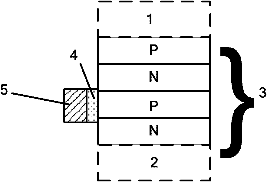
[0031] figure 1 It is a structural schematic diagram of the vertical selection tube of the embodiment of the present invention. Such as figure 1As shown, the vertical selection transistor includes an upper electrode 1 ; a lower electrode 2 ; and a semiconductor body region 3 formed between the upper electrode 1 and the lower electrode 2 . Wherein, the semiconductor body region 3 includes a first semiconductor layer, a second semiconductor layer, a third semiconductor layer, and a fourth semiconductor layer vertically stacked sequential...


PUM


Abstract

The invention provides a three-dimensional storage device array structure and a manufacturing method thereof. The three-dimensional storage array is formed by the derivation of grid control PNPN vertical selection tubes connected in series mutually and a storage cell of a resistant transformation or phase transformation cell in a three-dimensional space. The cross interference and leakage of electricity problems between adjacent units of the storage array in operation are improved effectively through the storage cell with high switching current ratio, also the structure of the storage cell issimplified, the multi-layer stacking is realized, and the storage density is improved.

Description

technical field [0001] The invention relates to the field of semiconductor design and manufacturing methods, in particular to a three-dimensional memory array structure based on gate-controlled PNPN vertical selection transistors and a manufacturing method thereof. Background technique [0002] Resistive RAM (RRAM) and Phase Change Memory (PCM), as a new type of non-volatile storage technology, due to its high storage density, low power consumption, fast read and write speed, long data retention time, multi-value realization, cell area, Compatibility with CMOS technology and other superior performance has attracted much attention. Among them, resistive memory and phase-change memory that can realize three-dimensional integration have become the research focus of high-density memory. At present, the most concerned structure is the multilayer stacked crossbar structure, but the multilayer stacked structure of the three-dimensional memory leads to crosstalk, leakage current, a...

Claims


Application Information

Patent Timeline
IPC IPC(8): H01L27/24H01L45/00
Inventor 潘立阳袁方
Owner XIAMEN IND TECH RES INST CO LTD
Why Eureka
Try Eureka