Method for casting crystal by seed crystal induction

A seed crystal and crystal technology, applied in the field of polycrystalline and single crystal semiconductor materials, to achieve the effects of low cost, high photoelectric efficiency and high production efficiency

Inactive Publication Date: 2012-01-11
赵钧永
View PDF7 Cites 18 Cited by
  • Summary
  • Abstract
  • Description
  • Claims
  • Application Information

AI Technical Summary

Problems solved by technology

The specific method is to use the seed crystal induction method. In the VGF, VB or BVS method, a silicon single crystal seed crystal is placed

Method used


Image

  • Method for casting crystal by seed crystal induction
  • Method for casting crystal by seed crystal induction
  • Method for casting crystal by seed crystal induction

Examples


Example Embodiment

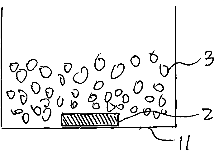
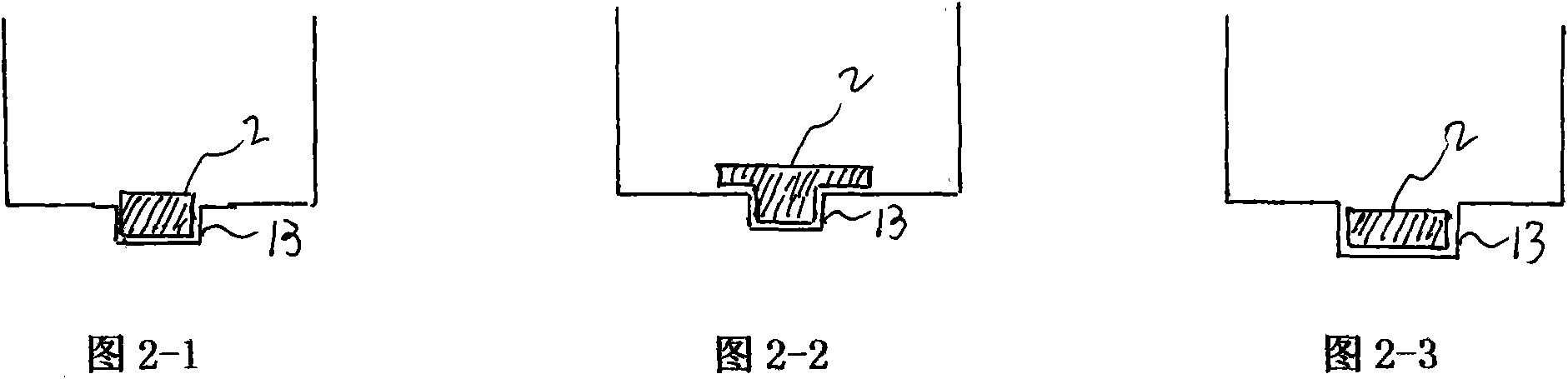
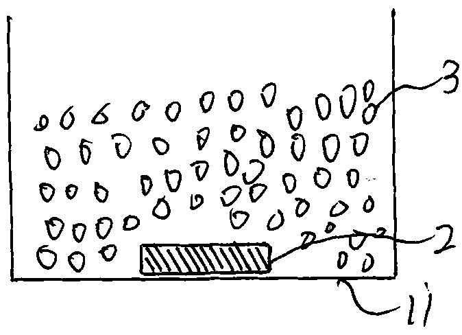
[0046] figure 1 In the method of the present invention of the silicon crystal manufacturing device using the silicon crystal growth process of the VGF method, the seed crystal is arranged at the bottom of the crucible. Wherein, the single crystal seed crystal plate 2 covers part of the inner surface of the bottom 11 of the crucible. The silicon raw material 3 is filled and covered above the seed crystal plate and other spaces in the crucible. The figure shows that the silicon raw material at the bottom of the crucible close to the seed crystal is preferably a small-sized granular or massive raw material. In this embodiment, the seed crystal plate can be fixed on the bottom of the crucible by, for example, welding or placing it directly.

[0047] To implement the method of the present invention, the heater is first activated to form a longitudinal temperature gradient in the crucible. Among them, the temperature near the horizontal plane at the lowest part of the crucible under t...


PUM


Abstract

The invention relates to a crystal material with a bigger size, which is manufactured by using a seed crystal induction vertical directional solidification casting method, in particular to a polycrystal or monocrystal material suitable for photoelectric application, such as silicon or silicon germanium. A traditional seed crystal used for casting a silicon crystal has a bigger size and higher consumption, thus, the invention provides a seed crystal with a smaller size and lower consumption, a method of casting a polycrystal or a monocrystal with the bigger size by using the seed crystal and the directional solidification method, the crystal material obtained by adopting the method, including a semiconductor crystal, and an application of the seed crystal in manufacturing semiconductor devices.

Description

Technical field [0001] The present invention generally relates to a vertical direction solidification casting method using seed crystal induction, such as vertical temperature gradient solidification crystal growth method (hereinafter also referred to as VGF method) or vertical Bridgman crystal growth method (hereinafter also referred to as VB method) or vertical The Bridgman Stockbadger method (VBS method) manufactures relatively large-sized crystalline materials, especially polycrystalline and single-crystalline semiconductor materials such as silicon or silicon germanium suitable for photovoltaic applications. Background technique [0002] Crystalline silicon-based photovoltaic cells (or photovoltaic cells, solar cells) should have the greatest possible efficiency in converting solar radiation power into current, as well as the longest possible service life and decay rate. This is determined by many factors, such as the purity of the silicon raw material, the type of silicon c...

Claims


Application Information

Patent Timeline
IPC IPC(8): C30B11/00
Inventor 赵钧永
Owner 赵钧永
Why Eureka
Try Eureka