Luminous device with superlattice structure active layer

A light-emitting device and superlattice technology, applied in semiconductor devices, electrical components, circuits, etc., can solve the problems of low luminous efficiency of light-emitting devices, improve crystal quality and luminous efficiency, reduce crystal defect density, improve stability and reliability effect

Active Publication Date: 2014-03-12
BYD SEMICON CO LTD
View PDF2 Cites 0 Cited by
  • Summary
  • Abstract
  • Description
  • Claims
  • Application Information

AI Technical Summary

Problems solved by technology

[0003] In order to solve the technical problem of low luminous efficiency of light emitting devices in the prior art, the present invention provides a light emitting device with a superlattice active layer

Method used


Image

  • Luminous device with superlattice structure active layer
  • Luminous device with superlattice structure active layer
  • Luminous device with superlattice structure active layer

Examples


Embodiment 1

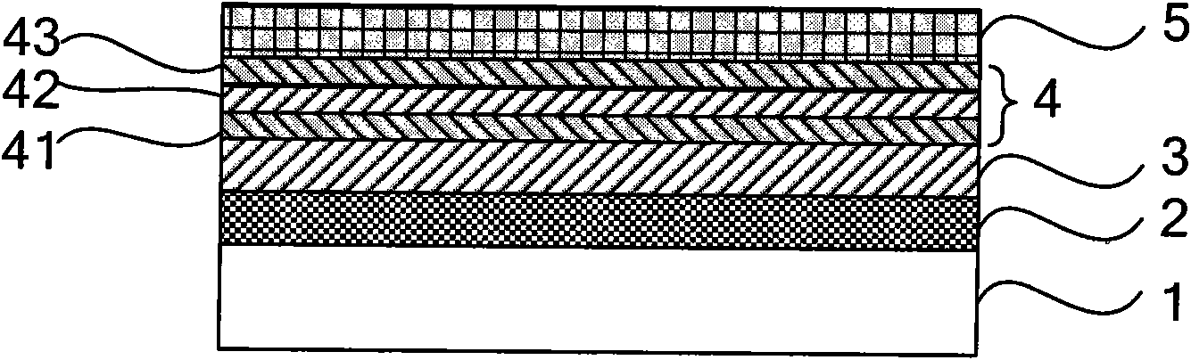
[0017] figure 2 It is a structural schematic diagram of the light-emitting device of Embodiment 1 of the present invention.

[0018] refer to figure 2 , a light emitting device according to Embodiment 1 of the present invention is proposed, and the light emitting device in this embodiment is a superlattice single quantum well light emitting device. The light-emitting device includes a sapphire substrate 100, a buffer layer 200 formed on the sapphire substrate 100 (the material of the buffer layer 200 is a gallium nitride semiconductor layer, also called a gallium nitride buffer layer 200), and a buffer layer 200 formed on the buffer layer 200. The first semiconductor layer 300 (also called N-type gallium nitride semiconductor layer 300), the first superlattice semiconductor layer 600 formed on the first semiconductor layer 300, and the organic layer formed on the first superlattice semiconductor layer 600 The source layer 400 (also called superlattice quantum well layer 40...

Embodiment 2

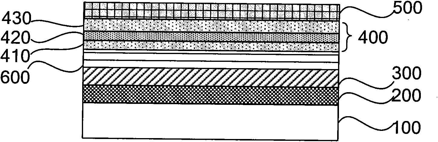
[0036] image 3 It is a structural schematic diagram of the light emitting device of the second embodiment of the present invention.

[0037] refer to image 3 , the light-emitting device of the second embodiment of the present invention is proposed. The light-emitting device in this embodiment is proposed on the basis of the light-emitting device in Embodiment 1, and the light-emitting device includes a sapphire substrate 100, a buffer layer 200 formed on the sapphire substrate 100, a first buffer layer 200 formed on the buffer layer 200 A semiconductor layer 300, a first superlattice semiconductor layer 600 formed on the first semiconductor layer 300, an active layer 400 formed on the first superlattice semiconductor layer 600, and a first superlattice semiconductor layer formed on the active layer 400 Two semiconductor layers 500, wherein the active layer 400 includes a first barrier layer 410, a superlattice potential well layer 420 formed on the first barrier layer 410,...

Embodiment 3

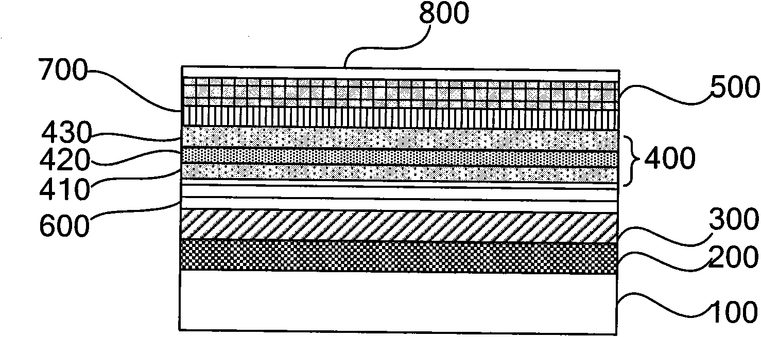
[0040] Figure 4 It is a structural schematic diagram of a light emitting device according to Embodiment 3 of the present invention.

[0041] This embodiment is proposed on the basis of the second embodiment, and the difference from the light-emitting device of the second embodiment lies in the superlattice quantum well layer. The superlattice quantum well layer in this embodiment is a superlattice multiple quantum well layer. The so-called superlattice multiple quantum well layer means that the superlattice quantum well layer has multiple superlattice potential well layers. The superlattice multiple quantum well layer 400 includes alternately stacked potential barrier layers and superlattice potential well layers. The superlattice multiple quantum well layer 400 includes multiple potential barrier layers and multiple superlattice potential well layers. In this embodiment, the barrier layer of the superlattice multi-quantum well layer 400 is preferably connected to the secon...


PUM


Abstract

The invention provides a luminous device with a superlattice structure active layer, which comprises a substrate and a multilayer III-V group nitride semiconductor structure, wherein the semiconductor structure is formed on the substrate and comprises a first semiconductor layer, an active layer and a second semiconductor layer which are sequentially formed on the substrate, the active layer comprises a superlattice quantum well layer, and the superlattice quantum well layer comprises a potential barrier layer and a superlattice potential well layer. Through the superlattice structure, the crystal defect density of the active layer and the piezoelectric polarization effect generated caused by the lattice dismatching of the active layer can be reduced, the crystal quality and the luminous efficiency of the active layer are improved, and the stability and the reliability of the luminous device are also improved.

Description

technical field [0001] The invention belongs to the technical field of solid-state semiconductor lighting, in particular to a light-emitting device with an active layer of a superlattice structure. Background technique [0002] Semiconductor light-emitting devices include light-emitting diodes, laser tubes, and the like. Now, light-emitting diodes have become the leading products of energy-saving lighting, and have received widespread attention worldwide. After the painstaking and excellent research and development of researchers, the luminous efficiency of the current light-emitting diodes has been greatly improved. refer to figure 1 At present, the main structure of the light-emitting diode includes a sapphire substrate 1, a gallium nitride (GaN) buffer layer 2 formed on the sapphire substrate 1, an N-type gallium nitride semiconductor layer formed on the gallium nitride buffer layer 2 3. The active layer 4 formed on the N-type gallium nitride semiconductor layer 3 and ...

Claims


Application Information

Patent Timeline
Patent Type & Authority Patents(China)
IPC IPC(8): H01L33/04
Inventor 苏喜林谢春林胡红坡张旺
Owner BYD SEMICON CO LTD
Why Eureka
Try Eureka