N type organic thin-film transistor and manufacturing method thereof

An organic thin film and transistor technology, applied in the field of N-type organic thin film transistors and their preparation, can solve the problems of limiting the development of transistors, short lifespan, and deteriorating device performance, and achieves improving carrier mobility, improving transmission capacity, and improving The effect of stability

Inactive Publication Date: 2012-01-25
UNIV OF ELECTRONICS SCI & TECH OF CHINA
View PDF4 Cites 8 Cited by
  • Summary
  • Abstract
  • Description
  • Claims
  • Application Information

AI Technical Summary

Problems solved by technology

[0008] Field-effect mobility is one of the most important performance indicators of transistors. After people's continuous efforts, the mobility of N-type OTFT has changed from the original 10 -4 cm 2 / Vs increased to 6 cm 2 / Vs, but compared with inorganic polycrystalline or single crystal field effect transistors, this value is still very small, which greatly limits the application of N-type organic thin film transistors
In addition, common N-type organic semiconductor materials are easily affected by water vapor or oxygen when operated in air, resulting in degraded device performance and short lifetime.
Most of the current N-type organic thin film transistors must be operated in nitrogen or vacuum, which greatly limits the further development of transistors

Method used


Image

  • N type organic thin-film transistor and manufacturing method thereof
  • N type organic thin-film transistor and manufacturing method thereof
  • N type organic thin-film transistor and manufacturing method thereof

Examples


Embodiment 1

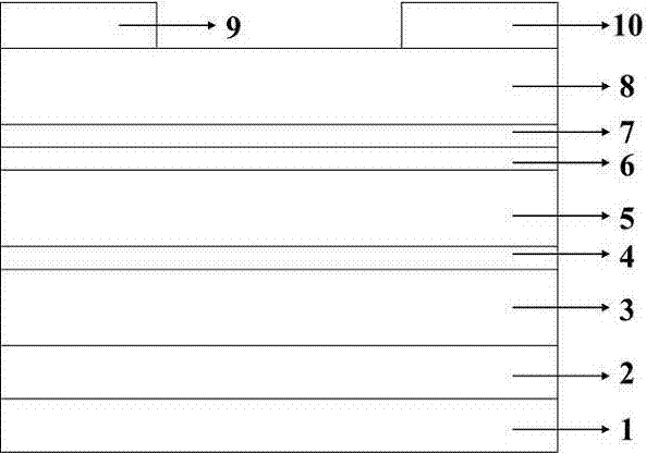
[0055] Device structure such as figure 1 shown. The material and thickness of each layer of the device are: substrate 1 is glass, gate electrode 2 is ITO, gate insulating layer 3 is PMMA (500 nm), two layers of modification layer are pentacene (2 nm), two layers of organic semiconductor The layers are all C60 (25 nm), the carrier blocking layer 6 is TAPC (2 nm), and the source electrode 9 and drain electrode 10 are both Ag (50 nm).

[0056] The preparation method of the organic thin film transistor is as follows:

[0057] ① Thoroughly clean the sputtered ITO glass substrate first, and dry it with dry nitrogen after cleaning;

[0058] ②Using the spin coating method to prepare PMMA film on ITO to form gate insulating layer;

[0059] ③Heating and baking the spin-coated PMMA film;

[0060] ④ Prepare the pentacene modified layer by vacuum evaporation;

[0061] ⑤ Prepare the first layer of C60 organic semiconductor layer by vacuum evaporation;

[0062] ⑥The TAPC carrier blocki...

Embodiment 2

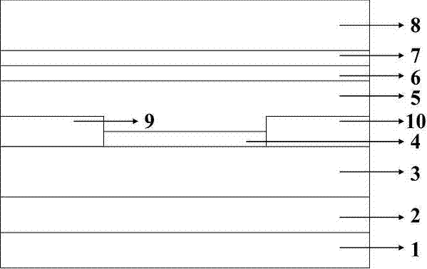
[0068] Device structure such as figure 1 shown. The material and thickness of each layer of the device are: substrate 1 is glass, gate electrode 2 is ITO, gate insulating layer 3 is PVP (2000 nm), two layers of modification layer are pentacene (5 nm), two layers of organic semiconductor The layers are all C60 (80 nm), the carrier blocking layer 6 is TAPC (10 nm), and the source electrode 9 and drain electrode 10 are both Ag (150 nm).

[0069] The fabrication process of the transistor is similar to that of Example 1.

Embodiment 3

[0071] Device structure such as figure 1 shown. The material and thickness of each layer of the device are: substrate 1 is glass, gate electrode 2 is ITO, gate insulating layer 3 is PVP (1000 nm), two layers of modification layer are pentacene (3 nm), two layers of organic semiconductor The layers are all C60 (100 nm), the carrier blocking layer 6 is TCTA (20 nm), and the source electrode 9 and drain electrode 10 are both Mg (300 nm).

[0072] The fabrication process of the transistor is similar to that of Example 1.


PUM


Abstract

The invention discloses an N type organic thin-film transistor and a manufacturing method thereof. The transistor comprises a substrate, a gate electrode, a gate insulation layer, a decorative layer, an organic semiconductor layer, a source electrode and a drain electrode, wherein the organic semiconductor layer comprises a first organic semiconductor layer and a second organic semiconductor layer made of N type organic semiconductor materials, and a current carrier barrier layer and the decorative layer are arranged between the first organic semiconductor layer and the second organic semiconductor layer. In the N type organic thin-film transistor, the current carrier barrier layer is introduced, thereby forming two channels on a device, reducing the phenomena of impacting, scattering and quenching of current carriers under a high biasing condition, and increasing the migration rate of the current carriers of the device; the decorative layer is introduced, thereby causing the organic semiconductor layer to have a better surface appearance, providing a better contact surface and promoting the transmission capability of current carriers in the channels; and a multilayer structure has a protection function, thereby promoting the stability of the transistor under an atmospheric environment.

Description

technical field [0001] The invention relates to the technical field of electronic components, in particular to an N-type organic thin film transistor and a preparation method thereof. Background technique [0002] Since the first organic thin film transistors (OTFT) were reported by Tsumura et al. in 1986, organic thin film transistors have been widely used due to their potential application value in active matrix display, organic integrated circuits, electronic trademarks and sensors. received widespread attention. It can be predicted that organic thin film transistors can greatly improve the current situation in the field of electronic information composed of field effect transistors in many aspects. Compared with inorganic transistors, organic thin film transistors have the following advantages: [0003] ①The organic thin film technology is more and newer, which makes the size of the device smaller and the integration level higher, so that the electronic components usin...

Claims


Application Information

Patent Timeline
Patent Type & Authority Applications(China)
IPC IPC(8): H01L51/05H01L51/40
Inventor 于军胜蔡欣洋于欣格蒋亚东
Owner UNIV OF ELECTRONICS SCI & TECH OF CHINA
Why Eureka
Try Eureka