Manufacturing method of flexible multi-layer circuit board

A technology of multi-layer circuit board and manufacturing method, which is applied in the field of circuit board manufacturing, and can solve problems such as defective circuit board products, failure of via holes, and different degrees of erosion between the adhesive layer and the substrate layer.

Active Publication Date: 2012-02-01
AVARY HLDG (SHENZHEN) CO LTD +1
View PDF5 Cites 11 Cited by
  • Summary
  • Abstract
  • Description
  • Claims
  • Application Information

AI Technical Summary

Problems solved by technology

Therefore, when mechanical drilling is used on a four-layer substrate, the adhesive layer and the substrate layer will change in different shapes under the high-speed rotation of the mechanical drill, resulting in poor drilling.
When laser drilling is used on a four-layer substrate, the degree of erosion between the adhesive layer and the substrate layer will be different due to the different absorption of laser energy by the adhesive layer and the substrate layer, which will also lead to poor drilling.
In this way, it may lead to the failure of the via hole, resulting in defective circuit board products.

Method used


Image

  • Manufacturing method of flexible multi-layer circuit board
  • Manufacturing method of flexible multi-layer circuit board
  • Manufacturing method of flexible multi-layer circuit board

Examples


Embodiment Construction

[0049] The method for manufacturing the flexible multilayer circuit board provided by the technical solution will be further described in detail below in conjunction with the accompanying drawings and multiple embodiments.

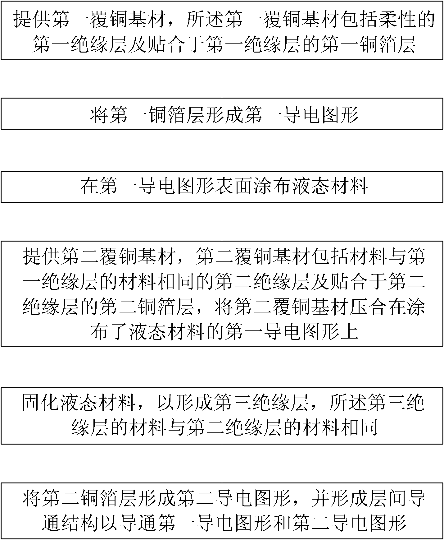
[0050] see figure 1 , the technical solution provides a method for manufacturing a flexible multilayer circuit board, comprising steps:

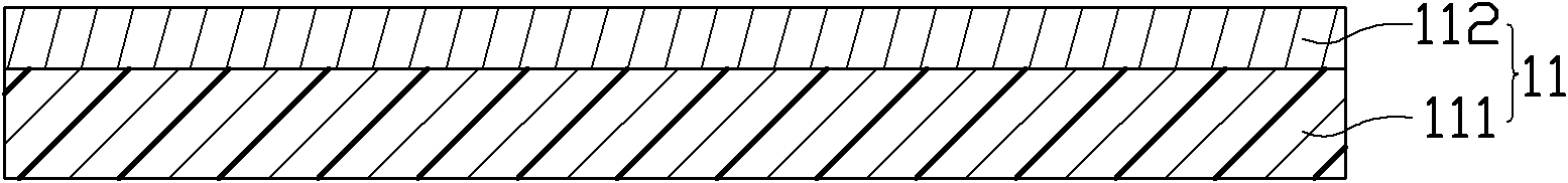
[0051] The first step is to provide a flexible first copper-clad substrate, the first copper-clad substrate includes a first insulating layer and a first copper foil layer bonded to the first insulating layer. The material of the first insulating layer is a flexible material, such as polyimide (Polyimide, PI), polyethylene terephthalate (PolyethyleneTerephthalate, PET) or polyethylene naphthalate (Polyethylene naphthalate). , PEN). The first copper foil layer may preferably be rolled copper foil, but may also be electrolytic copper foil.

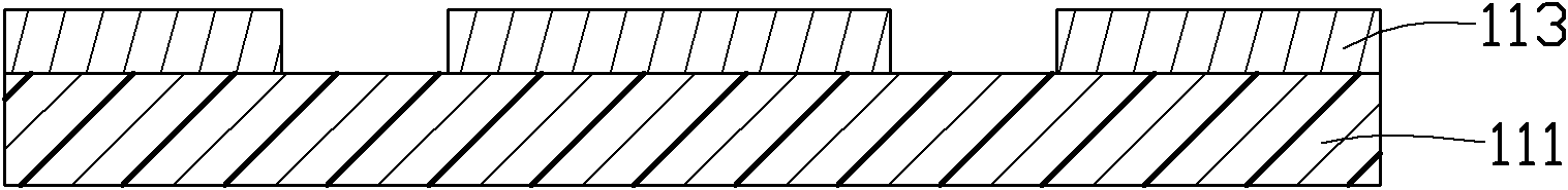
[0052] In the second step, the first copper foil layer is etched to form a firs...


PUM


Abstract

The invention provides a manufacturing method of a flexible multi-layer circuit board, which comprises the steps that: a first flexible copper clad laminate is provided, and the first copper clad laminate comprises a first insulation layer and a first copper foil layer; the first copper foil layer is formed into a first conductive pattern; a liquid material is applied on the surface of the first conductive pattern; a second copper clad laminate which comprises a second insulation layer and a second copper foil layer is provided, the material of the second insulation layer is the same with that of the first insulation layer, the second copper clad laminate is pressed on the first conductive pattern, and the second insulation layer is contacted with the liquid material; the liquid material is cured so that a third insulation layer is formed, and the material of the third insulation layer is the same with that of the second insulation layer; and the second copper foil layer is formed into a second conductive pattern, and an interlamination communicating structure is formed to communicate the first conductive pattern with the second conductive pattern. The materials of the insulation layers in the multi-layer circuit board which is manufactured through the method are same, so that the adverse conditions when communicating holes are manufactured can be avoided.

Description

technical field [0001] The invention relates to circuit board manufacturing technology, in particular to a method for manufacturing a flexible multilayer circuit board with better performance. Background technique [0002] With the wide application of flexible materials such as polyimide films in the electronic industry (see Sugimoto, E. "Applications of polyimide films to the electrical and electronic industries" published in IEEE Electrical Insulation Magazine, Vol. 5, No. 1, 1989 inJapan"), flexible printed circuit board (Flexible Printed Circuit Board, FPCB) is widely used in notebook computers, liquid crystal displays, digital cameras, mobile phones, etc. Electronic products have a very wide range of applications. With the improvement of people's requirements for processing information of consumer electronics products, because the multilayer circuit board has multilayer circuit layers and thus has more wiring area, the flexible multilayer circuit board gradually replac...

Claims


Application Information

Patent Timeline
Patent Type & Authority Applications(China)
IPC IPC(8): H05K3/46
Inventor 李明
Owner AVARY HLDG (SHENZHEN) CO LTD
Why Eureka
Try Eureka