
Antifuse device

A technology of anti-fuse and components, which is applied in the direction of electrical components, electric solid-state devices, semiconductor devices, etc., can solve problems such as difficult effects, achieve the effect of stable resistance value and ensure reliability

Inactive Publication Date: 2012-02-01
MURATA MFG CO LTD
View PDF6 Cites 6 Cited by
  • Summary
  • Abstract
  • Description
  • Claims
  • Application Information

AI Technical Summary

Problems solved by technology

[0014] Therefore, even if the antifuse element of Patent Document 2 for FPGA applications is applied to the application of countermeasures against open circuits of electronic components, it is difficult to sufficiently exhibit the expected effect.

Method used


Image

  • Antifuse device
  • Antifuse device
  • Antifuse device

Examples


Embodiment 1

[0145] According to the production method described in the above-mentioned first embodiment, a sample in which the trigger voltage was set to 20V was produced. However, when the electrostatic capacitance is measured at 1 kHz, it is 0.015 μF.

[0146] Table 1 shows the forming material, film thickness, and forming method of each layer.

[0147] [Table 1]

[0148]

[0149] Next, the sample was connected to a constant current circuit whose maximum current was set to 300 mA, and the resistance value after operation was measured. As a result, it was found that the average value of the resistance value was 1.2Ω (maximum 1.7Ω, minimum 0.7Ω, n: 20), and the operation was stable. In addition, it was confirmed that the resistance value did not change even when the maximum current was changed from 50 mA to 1.0 A.

[0150] Next, with respect to the above-mentioned sample, the cross-section of the sample at the welding position where the first electrode film and the second electrode ...

Embodiment 2

[0157] According to the production methods described in the second embodiment and the third embodiment, samples of Example 2 and Example 3 in which the trigger voltage was set to 20V were produced, respectively. However, production was performed under the same manufacturing conditions as in Example 1 except that the number of laminations of the element main body was increased (see Table 1 of Example 1).

[0158] In addition, when the electrostatic capacitance was measured at 1 kHz, it was 0.030 μF in Example 2 and 0.045 μF in Example 3. (The capacitance of Example 1 is 0.015 μF as described above).

[0159] Next, each sample of Examples 2 and 3 was connected to a constant current circuit with a maximum current of 300 mA, and the resistance value after operation was measured. However, the measurement was performed for each of 20 samples, and the average value was calculated.

[0160] Next, a machine model was prepared for 12 samples of each example, and the maximum voltage fo...


PUM

PropertyMeasurementUnit
thicknessaaaaaaaaaa
thicknessaaaaaaaaaa
thicknessaaaaaaaaaa

Abstract

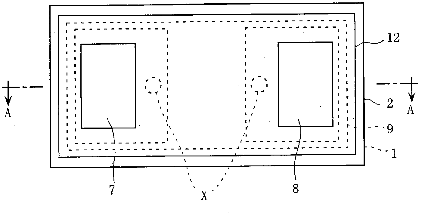
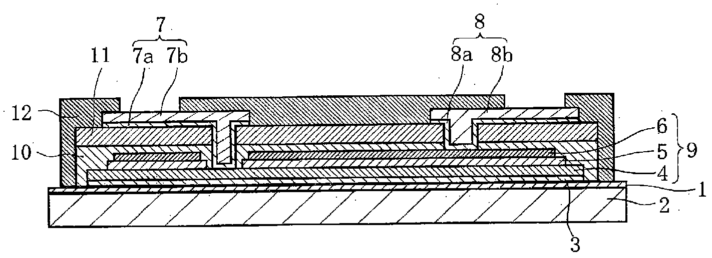
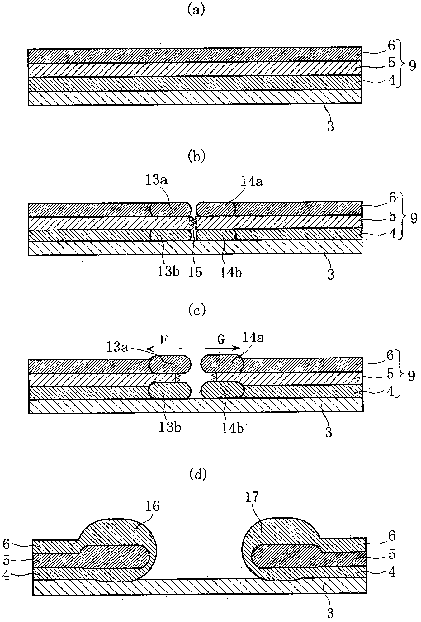
A device body (9) is formed by forming first and second electrode films (4, 6) on the top and bottom surfaces of a dielectric thin film (5)(a). When operating voltage is applied, the heat generated by the current flow causes the first and second electrode films (4, 6) to melt, forming ball parts (13a, 13b, 14a, 14b) and creating a crack (15) in the dielectric thin film (5) as well (b). Further, as the ball parts expand, the dielectric thin film (5) becomes completely divided (c) and the first and second electrode films (4, 6) fuse together in a manner that engulfs the ends of the dielectric thin film (5), thereby forming joined parts (16, 17) and establishing a state of electrical continuity (d). Due to this, after operation, the antifuse device can stably operate with low resistance even when high current is passing, and before operation, can function as an ESD counter device.

Description

technical field [0001] The present invention relates to an antifuse element (antifuse device), and more specifically, relates to parallel connection with electronic components and electronic equipment, and forms a bypass circuit (bypass circuit) by applying an overvoltage to irreversibly change from high resistance to low resistance the antifuse element. Background technique [0002] A plurality of light emitting diodes (Light Emitting Diodes; hereinafter referred to as “LEDs”) are mounted as light emitting sources on liquid crystal display devices and various lighting devices. [0003] In addition, in various electronic devices in recent years, many electronic components such as Zener diodes and varistors are mounted on an electronic circuit board. [0004] Furthermore, when such a plurality of electronic components are connected in series, a compensating element called an anti-fuse element is connected in parallel to each electronic component so that even if a specific el...

Claims


Application Information

Patent Timeline
Patent Type & Authority Applications(China)
IPC IPC(8): H01L21/82H05B37/03
CPCH01L25/167H01L25/0756H01L2224/32225H01L23/62H05B37/03H01L2924/0002H01L33/0095H01L23/5252H05B47/20H05B47/25H01L21/82
Inventor 中矶俊幸竹岛裕
Owner MURATA MFG CO LTD
Learn More