Quad flat non-leaded package structure and method of micro electro mechanical system device

A micro-electro-mechanical system and leadless packaging technology, applied in the field of micro-electro-mechanical systems, can solve problems such as simultaneous manufacturing and completion, and achieve the effects of small product size, superior performance, and good heat dissipation

Active Publication Date: 2012-02-08
嘉盛半导体(苏州)有限公司
View PDF5 Cites 20 Cited by
  • Summary
  • Abstract
  • Description
  • Claims
  • Application Information

AI Technical Summary

Problems solved by technology

[0005] Usually, MEMS devices need to use ASIC (Application Specific Integrated Circuits, Application Specific Integrated Circuits) chips to achieve specific functions. However, due to the large difference between the manufacturing process of MEMS devices and the manufacturing process of ASICs, it is impossible to use CMOS (Complementary Metal Oxide Semiconductor, complementary metal Oxide Semiconductor) Wafer Manufacturing Process Completed Simultaneously

Method used


Image

  • Quad flat non-leaded package structure and method of micro electro mechanical system device
  • Quad flat non-leaded package structure and method of micro electro mechanical system device
  • Quad flat non-leaded package structure and method of micro electro mechanical system device

Examples


Embodiment Construction

[0061] In order to make the objectives, technical solutions, and advantages of the embodiments of the present invention clearer, the following describes the embodiments of the present invention in further detail with reference to the accompanying drawings. Here, the exemplary embodiments of the present invention and the description thereof are used to explain the present invention, but not as a limitation to the present invention.

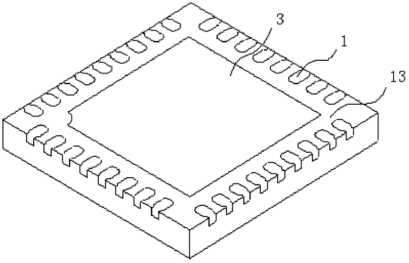
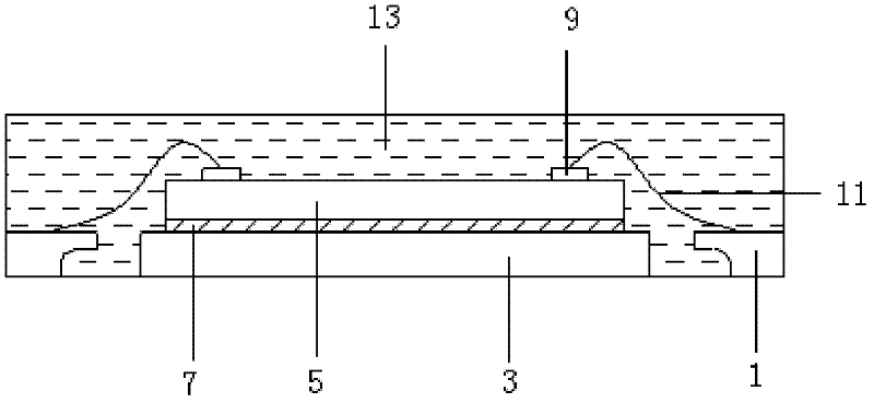
[0062] Picture 11 with Picture 12 It is a schematic diagram of a specific embodiment of the OFN structure of the MEMS device in the embodiment of the present invention. Figure 13 with Picture 14 It is a schematic diagram of another specific embodiment of the OFN structure of the MEMS device in the embodiment of the present invention. reference Figure 11 to Figure 14 The OFN structure of the MEMS device in the embodiment of the present invention may include:

[0063] Substrate

[0064] ASIC chip 20 pasted on the substrate;

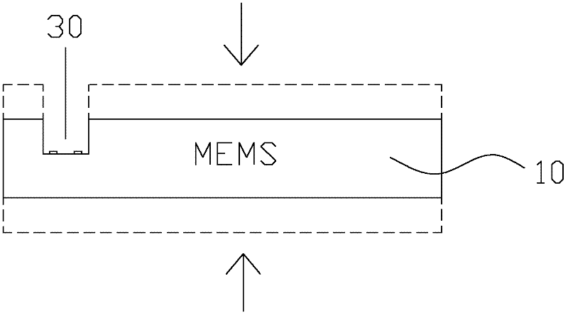
[0065] MEMS chip 10 paste...


PUM


Abstract

The invention discloses a quad flat non-leaded (QFN) package structure and a quad flat non-leaded package method of a micro electro mechanical system (MEMS) device. The structure comprises a substrate, an application specific integrated circuit (ASIC) chip, an MEMS chip and a plastic material, wherein the ASIC chip is adhered to the substrate; the MEMS chip is adhered to the ASIC chip; the substrate, the ASIC chip and the MEMS chip are packaged and a lead on the substrate is exposed by the plastic material; a micro bonding pad on the ASIC chip is connected with a lead on the substrate through a lead wire; a micro bonding pad on the MEMS chip is connected with the micro bonding pad on the ASIC chip through a lead wire; and on the ASIC chip, the micro bonding pad which is connected with the micro bonding pad on the MEMS chip is different from the micro bonding pad which is connected with the lead on the substrate. In the invention, the ASIC chip and the MEMS chip are packaged into an MEMS device with the ASIC chip by using a stacking mode; the method has the advantages of small product size, simple manufacturing process, superior performance and high heat dissipation performance; the conventional QFN production and manufacturing process can be utilized; and another choice is provided for packaging of the MEMS device.

Description

Technical field [0001] The present invention relates to the technical field of micro-electro-mechanical systems, in particular to a square flat no-lead packaging structure and method for micro-electro-mechanical system devices. Background technique [0002] MEMS (Micro Electro Mechanical systems) technology is a 21st century cutting-edge technology based on micro / nanotechnology. It refers to the design, processing, manufacturing, measurement and control of micro / nano materials technology. It can integrate mechanical components, optical systems, drive components, and electrical control systems into a micro system that is an integral unit. MEMS can not only collect, process and send information or instructions, but also take actions autonomously or according to external instructions according to the acquired information. It adopts a manufacturing process that combines microelectronics technology and micromachining technology to manufacture a variety of excellent performance, low ...

Claims


Application Information

Patent Timeline
Patent Type & Authority Applications(China)
IPC IPC(8): B81B7/00B81C3/00
CPCH01L2224/32145H01L2224/32245H01L2224/48145H01L2224/48247H01L2224/73265H01L2924/10155H01L2924/181H01L2924/00012H01L2924/00011
Inventor 吴斌尹丹陈群峰陈武伟
Owner 嘉盛半导体(苏州)有限公司
Why Eureka
Try Eureka