Ge-Sb-Te Ge-enriched N-doped phase-change material for phase-change memory and preparation method thereof

A phase change memory, ge-sb-te technology, applied in electrical components and other directions, can solve the problems of low crystalline resistivity and low crystallization temperature, and achieve the effects of grain refinement, high crystallization temperature, and reduced power consumption

Active Publication Date: 2012-02-08
SHANGHAI INST OF MICROSYSTEM & INFORMATION TECH CHINESE ACAD OF SCI
View PDF1 Cites 8 Cited by
  • Summary
  • Abstract
  • Description
  • Claims
  • Application Information

AI Technical Summary

Problems solved by technology

In phase change materials, Ge 2 Sb 2 Te 5 It is the most studied and most mature phase change material, which has the advantages of good electrical properties and good stability at high temperature, but it still cannot be considered as the best phase change material, and there are still some shortcomings, such as crystal state Low resistivity and low crystallization temperature, etc.

Method used


Image

  • Ge-Sb-Te Ge-enriched N-doped phase-change material for phase-change memory and preparation method thereof
  • Ge-Sb-Te Ge-enriched N-doped phase-change material for phase-change memory and preparation method thereof
  • Ge-Sb-Te Ge-enriched N-doped phase-change material for phase-change memory and preparation method thereof

Examples


Embodiment 1

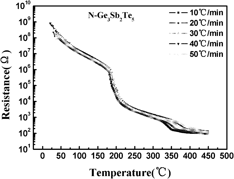
[0031] 1. The Ge-Sb-Te rich Ge-doped N thin film material was prepared on the silicon substrate and the thermally oxidized silicon substrate at the same time by magnetron sputtering two-target co-sputtering method, and the background vacuum degree was 1.6×10 -4 Pa, the argon gas pressure during sputtering is 0.22Pa, N 2 / Ar 2 The flow ratio is 1sccm / 49sccm, Ge target and Ge 2 Sb 2 Te 5 The sputtering power of the target is 20W for radio frequency and 30W for DC respectively, the sputtering rate is 10nm / min, and the sputtering time is 30min. The thickness of the prepared phase change film is 300nm observed by SEM, and the mole percentage of N element is 2.02 by XPS. %, EDS energy spectrum analysis shows that the composition of the material is N 2.02 (Ge 3 Sb 2 Te 5 ) 97.98 .

[0032] 2. The obtained N grown on the silicon oxide wafer without annealing 2.02 (Ge 3 Sb 2 Te 5 ) 97.98 The in-situ resistance test of the phase-change thin film material shows the relation...

Embodiment 2

[0036] 1. Prepare Ge-Sb-Te rich Ge-doped N film material N according to the magnetron sputtering method of embodiment 1 10 [(Ge 3 Te)(Sb 2 Te 3 ) 2 ] 90 : When using magnetron sputtering two-target co-sputtering method to sputter on silicon substrate and thermally oxidized silicon substrate at the same time, by adjusting N 2 / Ar 2 Flow ratio and Ge target and Ge 2 Sb 2 Te 5 The sputtering power of the target is obtained.

[0037] N in this example 10 [(Ge 3 Te)(Sb 2 Te 3 ) 2 ] 90 The thickness of the phase change film material is 300nm observed by SEM, the content of N element is 10% obtained by XPS, and the EDS energy spectrum analysis shows that the composition of the material is N 10 [(Ge 3 Te)(Sb 2 Te 3 ) 2 ] 90 .

[0038] 2. The N that was grown on the silicon oxide sheet and not annealed obtained in this embodiment 10 [(Ge 3 Te)(Sb 2 Te 3 ) 2 ] 90 The in-situ resistance test of the phase change thin film material, the relationship between the s...

Embodiment 3

[0042] 1. Prepare Ge-Sb-Te rich Ge-doped N film material N according to the magnetron sputtering method of embodiment 1 25 [(Ge 3 Te)(Sb 2 Te 3 )] 75 : When using magnetron sputtering two-target co-sputtering method to sputter on silicon substrate and thermally oxidized silicon substrate at the same time, by adjusting N 2 / Ar 2 Flow ratio and Ge target and Ge 2 Sb 2 Te 5 The sputtering power of the target is obtained.

[0043] N in this example 25 [(Ge 3 Te)(Sb 2 Te 3 )] 75 The thickness of the phase change film material is 300nm observed by SEM, the content of N element is 10% obtained by XPS, and the EDS energy spectrum analysis shows that the composition of the material is N 25 [(Ge 3 Te)(Sb 2 Te 3 )] 75 .

[0044] 2. The N that was grown on the silicon oxide sheet and not annealed obtained in this embodiment 25 [(Ge 3 Te)(Sb 2 Te 3 )] 75 The in-situ resistance test of the phase change thin film material, the relationship between the sheet resistance ...


PUM


Abstract

The invention relates to a Ge-Sb-Te Ge-enriched N-doped phase-change material for a phase-change memory. The Ge-Sb-Te Ge-enriched N-doped phase-change material for the phase-change memory, provided by the invention, comprises chemical components which accord with a chemical formula as follows: Nx[(Ge1+yTe)a(Sb2Te3)b]100-x, wherein y is more than 0 but not more than 3, x is more than 0 but not more than 35, a is equal to 1 or 2 and b is equal to 1 or 2. The phase-change material is a storage material which has a reversible phase change under the effects of external energy. When a magnetic control sputtering is adopted, atom percentage contents of all the components are adjusted through controlling a power supply power of each target material and each target position and the N2/Ar2 flow ratio so that phase-change storage materials with different crystallization temperatures, smelting points and crystallization activation energies are obtained. Compared with the traditional Ge2Sb2Te5 thin-film material, the Ge-enriched N-doped phase-change material provided by the invention has the advantages of higher crystallization temperature, better data keeping capability, better heat stability, lower power consumption and the like.

Description

technical field [0001] The invention relates to a phase change thin film material in the technical field of microelectronics, in particular to a phase change thin film material composed of a mixture of germanium-antimony-tellurium doped with nitrogen. Background technique [0002] Phase-change memory is a kind of memory that uses the change of material phase to realize information storage. It was first based on the Ovshinsky electronic effect discovered by S.R.Ovshinsky in chalcogenide compounds in the late 1960s. Phase change memory technology has been developing slowly until the size of the material in the device can be reduced to the nanometer level with the development of nano-fabrication technology and process, and the phase-change memory has developed rapidly. [0003] Phase-change memory uses phase-change materials to change reversibly between amorphous and crystalline states, and has a strong resistance contrast before and after the phase change to realize informatio...

Claims


Application Information

Patent Timeline
Patent Type & Authority Applications(China)
IPC IPC(8): H01L45/00
Inventor 宋志棠程丽敏吴良才饶峰刘波彭程
Owner SHANGHAI INST OF MICROSYSTEM & INFORMATION TECH CHINESE ACAD OF SCI
Why Eureka
Try Eureka