Pitted-surface metal and rubber composite conductive particle

A technology of conductive particles and metals, applied in circuits, electric switches, electrical components, etc., can solve the problems of inability to balance conductivity and strength, and achieve the effects of easy industrial production and batch application, controllable cost and reasonable structure

Active Publication Date: 2012-02-15
NANTONG MEMTECH TECH
View PDF8 Cites 61 Cited by
  • Summary
  • Abstract
  • Description
  • Claims
  • Application Information

AI Technical Summary

Problems solved by technology

[0006] Purpose of the invention: To overcome the defect that the conductivity and strength of traditional button conductive particles cannot be balanced, and to provide a pockmarked metal and rubber composite conductive particle that ensures reliable contact with the circuit and good conductivity

Method used


Image

  • Pitted-surface metal and rubber composite conductive particle
  • Pitted-surface metal and rubber composite conductive particle

Examples


Embodiment 1

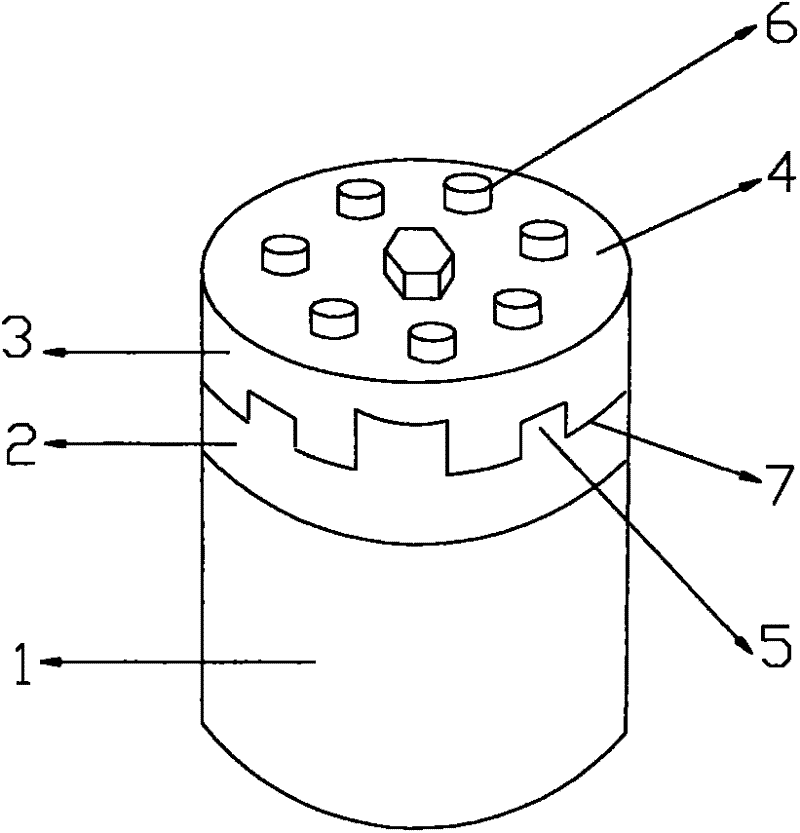
[0025] As shown in the drawings, the depth of the pits 5 is less than the thickness of the metal surface layer 1 , and the height of the bumps 6 is less than twice the thickness of the metal surface layer 1 . The maximum area of ​​the pits 5 and bumps 6 is 0.1mm 2 -1mm 2 ; The distance between the adjacent pits 5, between the bumps 6 or between the adjacent pits 5 and the bumps 6 is 0.05mm-0.5mm.

[0026] The distribution of the pits 5 or bumps 6 on the metal surface layer 1 is uniform. The metal surface layer 1 is circular, and the planar shape of the pits 5 or bumps 6 is circular. The metal surface layer 1 is made of 0.1 mm thick metal copper, and the outer surface 4 of the metal surface layer is also plated with 4 micron thick nickel, and then a layer of 1.5 micron hard gold is plated on the nickel. As an intermediate layer, the nickel plating acts as a barrier between gold and copper. It can prevent the mutual diffusion between gold and copper and prevent copper from pe...

Embodiment 2

[0029] As shown in the drawings, the depth of the pits 5 is smaller than the thickness of the metal surface layer 1 , and the height of the bumps 6 is smaller than the thickness of the metal surface layer 1 . The maximum area of ​​the pits 5 and bumps 6 is 0.5mm 2 -2mm 2 ; The distance between adjacent pits 5, adjacent bumps 6 or between adjacent pits 5 and bumps 6 is 0.5mm-1mm, ensuring reliable contact with the integrated circuit.

[0030] The distribution of the pits 5 or bumps 6 on the metal surface layer 1 is random, the metal surface layer 1 is heart-shaped, and the plane shape of the pits 5 or bumps 6 is ellipse.

[0031] The metal surface layer 1 is made of aluminum alloy, and the outer surface 4 of the metal surface layer is also plated with silver to increase electrical conductivity and corrosion resistance. The adhesive layer 2 is vulcanized rubber adhesive, the rubber matrix 3 is silicone rubber, and the adhesive layer 2 is embedded in the pit 5 of the metal surf...

Embodiment 3

[0033] As shown in the drawings, the height of the bumps 6 is less than twice the thickness of the metal surface layer 1 . The maximum area of ​​the planes of the pits 5 and bumps 6 is 1mm 2 -5mm 2 ; Between the adjacent pits 5 and between the adjacent bumps 6 are 1mm-2mm.

[0034] The distribution of the pits 5 or bumps 6 on the metal surface layer is regular. The metal surface layer 1 is a regular polygon, the planar shape of the pits 5 is irregular, and the planar shape of the bumps 6 is circular. The metal surface layer 1 is made of iron-nickel bimetallic composite material, the adhesive layer 2 is a thermally vulcanized rubber adhesive layer, and the rubber matrix 3 is silicone rubber.

[0035] Before the metal surface layer 1 is bonded to the rubber substrate 3, the inner surface 7 of the metal surface layer is degreased by an organic solvent, and the bonding surface of the rubber substrate 3 is decontaminated by a synthetic washing liquid; the degreasing and decontamin...


PUM

PropertyMeasurementUnit
thicknessaaaaaaaaaa
areaaaaaaaaaaa

Abstract

The invention provides a pitted-surface metal and rubber composite conductive particle, which is formed by adhering a metal surface layer to a rubber basic body or slitting after adhesion, wherein the metal surface layer is a pitted surface and has pits or bumps or both the pits and the bumps; the pits or the bumps are formed on an external surface of the metal surface layer or an internal surface or both the external surface and the internal surface; the depths of the pits are smaller than the thickness of the metal surface layer; the heights of the bumps are greater than or equal to one tenth of the thickness of the metal surface layer; the metal surface layer is made of metal or alloy; gold, silver, copper or nickel can be coated on the external surface of the metal surface layer; the rubber basic body is made of silicon rubber or polyurethane rubber; an adhesion layer can be arranged between the metal surface layer and the rubber basic body; the adhesion layer is made of a heat vulcanization adhesive, a prime coating agent or a material which is the same as that of the rubber basic body; and aids such as a coupling agent can be coated on the internal surface of the metal surface layer. The metal surface layer is high in strength, stable in conductivity, high in strength of the adhesion layer and high in elasticity of the rubber basic body; and the pitted-surface metal and rubber composite conductive particles can serve as conductive parts of various kinds of keys of a mobile phone, an automobile and the like, and the cost can be controlled.

Description

technical field [0001] The invention relates to a conductive part for keys, in particular to a pitted metal and rubber composite conductive particle formed by compounding pitted metal foil or sheet and a rubber matrix. Background technique [0002] When all kinds of keys such as mobile phones, computers, calculators, and automobiles are installed and used, the back of the keys must be backed with elastic parts, so that the keys can have a better tactile feeling. Usually the elastic part is made of rubber, and the elastic part needs to be in contact with the integrated circuit so that the relevant circuit is turned on when the button is pressed. Since the conductivity of the rubber is not good, it is necessary to use conductive particles to increase the conductivity of the button and the contact of the circuit switch. [0003] The specification of patent application number 98117795.6 discloses a "conductive elastomer for joining to an elastic substrate". The conductive elas...

Claims


Application Information

Patent Timeline
Patent Type & Authority Applications(China)
IPC IPC(8): H01H13/02H01H1/04
Inventor 韩辉升张劲松顾建祥董亚东黄志宏黄诚
Owner NANTONG MEMTECH TECH
Why Eureka
Try Eureka