Lead-free LED (Light-Emitting Diode) module and manufacturing process thereof

A technology for LED modules and manufacturing processes, applied in electrical components, electrical solid-state devices, circuits, etc., can solve the problems of low thermal conductivity of intermediate layers, low optical transmittance, poor heat dissipation performance, etc., and achieve transmittance. High, low cost, the effect of improving the light output efficiency

Inactive Publication Date: 2012-02-29
HANGZHOU HPWINNER OPTO CORP
View PDF5 Cites 15 Cited by
  • Summary
  • Abstract
  • Description
  • Claims
  • Application Information

AI Technical Summary

Problems solved by technology

The above-mentioned LED module has the following defects: because the heat dissipation of the LED chip needs to pass through many interlayers in the heat conduction channel, and the medium between the LED heat sink and the PCB board 102, and the medium between the PCB board 102 and the radiator 101 is air or silicone grease. Vias have low thermal conductivity, so thermal performance is poor
[0007] For general LED application lamps, after the light is emitted from the chip, it generally passes through: phosphor, packaging lens, air, light distribution lens, and then to the light transmission cover. The light passes through many media, and reflection loss occurs at each interface, so the total low optical transmittance
Therefore, there are disadvantages such as poor heat dissipation performance, low optical transmittance, complicated production process, and high cost.

Method used


Image

  • Lead-free LED (Light-Emitting Diode) module and manufacturing process thereof
  • Lead-free LED (Light-Emitting Diode) module and manufacturing process thereof
  • Lead-free LED (Light-Emitting Diode) module and manufacturing process thereof

Examples


Embodiment

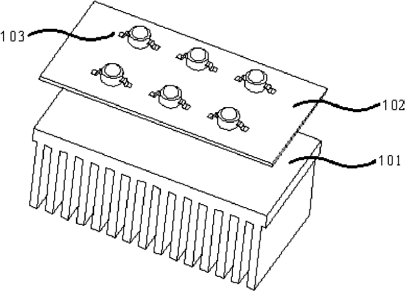
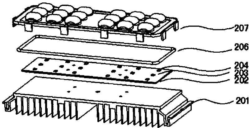
[0076] like figure 2 As shown, an LED module includes: a heat sink 201 , a PCB board 202 , an LED chip 203 , an LED open circuit protector 204 , encapsulating colloid, sealing silicone 206 , and a lens module 207 . In this embodiment, the LED open circuit protector 204 is a Zener diode. The sealing silicone 206 includes a solid silicone ring installed on the lens module 207, and a gel silicone ring formed by liquid silicone coated on the side of the solid silicone ring. On the position corresponding to the plane of the lens module 207 on the side of the solid silicone ring, there is a groove for coating liquid silicone. In the present embodiment, the lens module 207 has an overall plane, on the plane, it is obvious that each convex is a lens (if you look upside down, it is a lens pit), and the edge position around the plane is first attached with a Solid silicone ring, the outer or inner position of the solid silicone ring, corresponding to the plane of the lens module 207,...


PUM


Abstract

The invention relates to a lead-free LED (Light-Emitting Diode) module and a manufacturing process thereof. The LED module comprises a radiator, a PCB (Printed Circuit Board), an LED chip, an encapsulating colloid, sealing silica gel and a lens module, wherein the LED chip is welded on the PCB; the anode and cathode of the LED chip are welded on corresponding electrode pads respectively; the PCB is jointed with the radiator; and the lens module is arranged above the LED chip, and is filled with the encapsulating colloid. The LED chip is directly welded on the circuit board, so that the conventional LED encapsulating process is eliminated, a bracket comprising a heat sink is eliminated, heat of the LED chip is directly diffused to the high-heat-conductivity circuit board and the radiator, and the radiating effect is enhanced. Only the sealing colloid is arranged between the lens module and the LED chip, so that light rays pass through a small quantity of media, and the transmittance is high; and the filling colloid is matched with the refractive index of the lens module, so that the reflection loss is small, and the light emitting rate of the LED module is increased.

Description

technical field [0001] The invention relates to the field of semiconductor application and packaging, more specifically, to a leadless LED module and its manufacturing process. Background technique [0002] With the development of LED chip technology and packaging technology, more and more LED products are used in the field of lighting, especially high-power white LEDs. Due to the characteristics of high light efficiency, long life, energy saving and environmental protection, suitable dimming control, and no mercury and other pollutants, LEDs have become a new generation of lighting sources after traditional light sources such as incandescent lamps and fluorescent lamps. [0003] LED is an electroluminescent semiconductor device, in which about 30% of the electrical energy is converted into light, and the remaining electrical energy is converted into heat, and the temperature rise of LED caused by heat accumulation is the main cause of LED light decay. Therefore, LED chip h...

Claims


Application Information

Patent Timeline
Patent Type & Authority Applications(China)
IPC IPC(8): H01L25/075H01L33/48H01L33/64H01L33/00
Inventor 陈凯黄建明杨帆
Owner HANGZHOU HPWINNER OPTO CORP
Why Eureka
Try Eureka