Marking method for ingot casting polycrystalline silicon slice head and tail sequencing

A polysilicon and marking technology, which is applied in the direction of electrical components, circuits, semiconductor devices, etc., can solve the problems of a large number of fragments of silicon wafers and the inability to distinguish the exact position, etc.

Inactive Publication Date: 2012-02-29
TRINA SOLAR CO LTD
View PDF3 Cites 9 Cited by
  • Summary
  • Abstract
  • Description
  • Claims
  • Application Information

AI Technical Summary

Problems solved by technology

[0005] The technical problem to be solved by the present invention is to propose a marking method for the head-to-tail sorting of ingot polysilicon wafers, which overcomes the inability to identify the exact position of the silicon wafers in the ingot after processing and the silicon wafers being in the cutting process due to multiple markings. The problem with a lot of fragmentation in the process

Method used


Image

  • Marking method for ingot casting polycrystalline silicon slice head and tail sequencing
  • Marking method for ingot casting polycrystalline silicon slice head and tail sequencing

Examples


Embodiment Construction

[0019] The present invention will now be described in further detail in conjunction with the accompanying drawings and preferred embodiments. These drawings are all simplified schematic diagrams, which only illustrate the basic structure of the present invention in a schematic manner, so they only show the configurations related to the present invention.

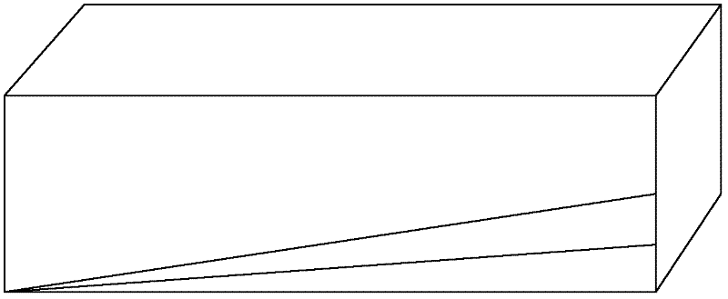
[0020] Firstly, the ingot polysilicon ingot after squaring is tested by infrared and minority carrier lifetime, and the truncation position is determined based on the infrared and minority carrier lifetime detection results, and the truncation process is carried out. Then use a laser to draw a line mark on the surface of the truncated ingot.

[0021] Specific identification methods such as figure 1 As shown in FIG. 1 , one surface of the truncated polysilicon rod is selected for laser line drawing. Draw a line from a vertex of the ingot head to its opposite side, the intersection point of the first line and the opposite si...


PUM


Abstract

The invention relates to a marking method for ingot casting polycrystalline silicon slice head and tail sequencing, which comprises the following steps: 1) detecting: carrying out infrared and minority carrier lifetime detection on a squarely holed ingot casting polycrystalline silicon crystal bar; 2) cutting off: determining the cut-off position according to the infrared and minority carrier lifetime detection results so as to carry out cut-off processing; 3) marking: utilizing laser to draw lines for marking on the surface of the cut-off crystal bar; 4) surface burnishing: burnishing the surface of the marked crystal bar for polishing; 5) chamfering: chamfering the crystal bar after surface burnishing; 6) bar sticking: sticking the chamfered crystal bar onto a crystal holder through curing adhesive; and 7) slicing: curing the crystal bar for a period of time and then sending the crystal bar into a stock for slicing. The ingot casting polycrystalline silicon bar is sliced after being marked in the method disclosed by the invention, and finally the heads and tails of silicon slices are sequenced according to the positions of line marks at the edges of the silicon slices, so the positions of the silicon slices in the crystal bar can be clearly identified, and the fragmentation rate is not increased.

Description

technical field [0001] The invention relates to a method for marking a silicon chip, in particular to a method for marking on the surface of a silicon ingot by using a laser. Background technique [0002] Since the 1970s, in view of the limited supply of conventional energy sources and the increasing pressure on environmental protection, many countries in the world have set off an upsurge in the development and utilization of solar energy. Because of its high reliability, long life, and ability to withstand various environmental changes, crystalline silicon solar cells have become the main variety of solar cells and dominate the photovoltaic market. In terms of its crystal form, there are three main categories: monocrystalline silicon, polycrystalline silicon and amorphous silicon. Monocrystalline silicon cells have high conversion efficiency and good stability, but the drawing process is relatively complicated, and the requirements for raw materials are strict, resulting i...

Claims


Application Information

Patent Timeline
Patent Type & Authority Applications(China)
IPC IPC(8): H01L31/18H01L21/00
Inventor 张驰刘振淮熊震付少永
Owner TRINA SOLAR CO LTD
Why Eureka
Try Eureka