Method for preparing Na-doped p-type NnO film
A thin-film, p-type technology, applied in the field of thin-film doping, can solve the problems of destroying the quality of ZnO thin films, being easily corroded, and affecting the purity of dopants.
- Summary
- Abstract
- Description
- Claims
- Application Information
AI Technical Summary
Problems solved by technology
Method used
Image

Examples
Embodiment 1
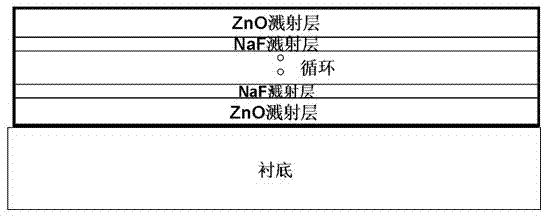
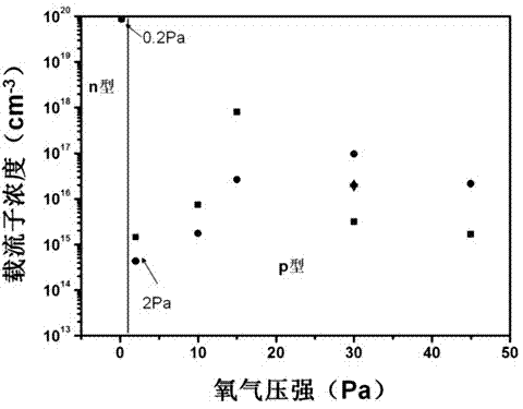
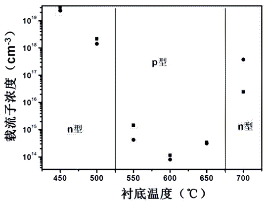
[0026] Take the following process steps: 1) Clean the sapphire substrate, put it into the growth chamber of the pulsed laser deposition device after cleaning, and pump the vacuum of the reaction chamber to 1×10 -4 Pa; then heat the substrate so that the substrate temperature is 400°C; adjust the oxygen pressure to 2Pa. First, pure ZnO was used as the target to sputter and deposit ZnO thin film for 90 s, and then the target was changed to pure NaF target for sputter growth for 10 s, and Na-doped ZnO thin film was prepared in this way for 20 cycles. The distance between the substrate and the target is 4.5 cm, the laser frequency is 3 Hz, and the laser energy is 250 mJ. After growth, cool down to room temperature at a rate of 3 °C / min. The Na-doped ZnO film on the sapphire substrate is n-type; 2) The Na-doped ZnO film on the sapphire substrate 2 Rapid annealing treatment at 400°C for 5 minutes in the atmosphere, so that Na ions diffuse in the ZnO film, and obtain p Type ZnO f...
Embodiment 2
[0029] Take the following process steps: clean the quartz substrate, put it into the growth chamber of the pulsed laser deposition device after cleaning, and pump the vacuum of the reaction chamber to 1.0×10 -3 Pa; then heat the substrate so that the substrate temperature is 550°C; adjust the oxygen pressure to 30Pa. First, pure ZnO was used as the target to sputter and deposit ZnO thin film for 90 s, and then the target was switched to pure NaF target for sputter growth for 10 s, and Na-doped ZnO thin film was prepared by 20 cycles of growth in this way. The distance between the substrate and the target is 5 cm, the laser frequency is 5 Hz, and the laser energy is 300 mJ. After growth, cool down to room temperature at a rate of 4 °C / min. Na-doped ZnO films were obtained. 2) As-prepared Na-doped ZnO thin film in N 2 Rapid annealing at 650°C for 5 minutes under atmosphere.
[0030] Carry out the Hall test, you can see that the test results show that the carrier type is p t...
Embodiment 3
[0033] Take the following process steps: clean the quartz substrate, put it into the growth chamber of the pulsed laser deposition device after cleaning, and pump the vacuum of the reaction chamber to 8.0×10 -4 Pa; then heat the substrate so that the substrate temperature is 550°C; adjust the oxygen pressure to 0.02Pa. First, pure ZnO was used as the target to sputter and deposit ZnO thin film for 90 s, and then the target was switched to pure NaF target for sputter growth for 10 s, and Na-doped ZnO thin film was prepared by 20 cycles of growth in this way. The distance between the substrate and the target is 5 cm, the laser frequency is 5 Hz, and the laser energy is 300 mJ. After growth, cool down to room temperature at a rate of 3 °C / min. 2) As-prepared Na-doped ZnO thin film in N 2 Rapid annealing at 650°C for 5 minutes under atmosphere. Na-doped ZnO films were obtained.
[0034] The prepared Na-doped ZnO film was tested by XPS, and it can be seen that the test results...
PUM
 Abstract
Description
Claims
Application Information
 - R&D
- Intellectual Property
- Life Sciences
- Materials
- Tech Scout
- Unparalleled Data Quality
- Higher Quality Content
- 60% Fewer Hallucinations
Browse by: Latest US Patents, China's latest patents, Technical Efficacy Thesaurus, Application Domain, Technology Topic, Popular Technical Reports.
© 2025 PatSnap. All rights reserved.Legal|Privacy policy|Modern Slavery Act Transparency Statement|Sitemap|About US| Contact US: help@patsnap.com