Liquid crystal exposure device

An exposure device and a technology for exposing patterns, which are applied in photolithography exposure devices, microlithography exposure equipment, optics, etc., can solve the problems of residual wrinkles on the substrate and the inability of the substrate to become flat, so as to ensure flatness and shorten production The effect of takt time

Inactive Publication Date: 2012-03-14
HITACHI HIGH-TECH CORP
View PDF5 Cites 4 Cited by
  • Summary
  • Abstract
  • Description
  • Claims
  • Application Information

AI Technical Summary

Problems solved by technology

When the substrate is placed on the chuck in a shape in which the central part is swollen by air, etc., even if the air in both is exhausted by a vacuum force of 200 through the vacuum region, the contact fri...

Method used


Image

  • Liquid crystal exposure device
  • Liquid crystal exposure device
  • Liquid crystal exposure device

Examples


Embodiment 1

[0077] use Figure 1 to Figure 7 A first embodiment of the present invention will be described.

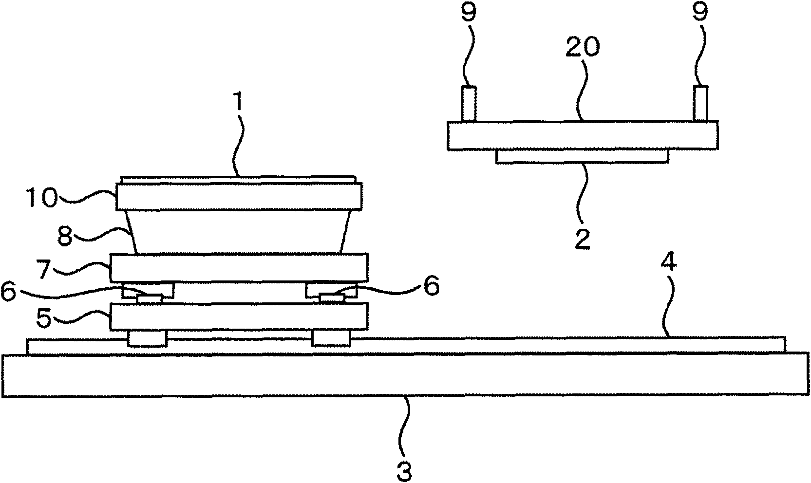
[0078] figure 1 It is a figure which shows the schematic structure of the exposure apparatus which concerns on one Embodiment of this invention. This embodiment shows an example of an exposure apparatus of a proximity method in which a minute gap (proximity gap) is provided between a mask and a substrate and a mask pattern is transferred to a substrate. The exposure device consists of the following components: base 3, X guide 4, X stage 5, Y guide 6, Y stage 7, θ stage 8, Z-tilt mechanism 9, chuck 10 and mask Die holder 20. In addition, the exposure apparatus includes a light source for exposure, a supply unit for supplying the substrate 1 to the chuck 10 , a recovery unit for recovering the substrate 1 from the chuck 10 , a temperature control unit for controlling the temperature inside the apparatus, and the like.

[0079] exist figure 1 In , the chuck 10 is at the transf...


PUM


Abstract

By adopting he method of contacting and supporting a chuck with a substrate in an exposure device, inside reversion of maintaining the substrate shape caused by dust adhered to the substrate can occur, and due to the contacting sequence of the substrate or the chuck, the substrate can be creased, the flatness can be damaged, and the exposure is bad. Thus, through a part which is arranged on the chuck and used for enabling the substrate to float with an air force, the substrate is maintained in a non-contact way, the flatness damage and creasing caused by the contact state can be prevented, and exposure images can be exposed on the substrate precisely. Moreover, through arranging a constant temperature part, the temperature change of the floating substrate can be prevented, and color inferiority caused by the floating exposure of the substrate can be avoided.

Description

technical field [0001] The present invention relates to exposure apparatus. For example, it is related with the manufacturing apparatus of the panel for liquid crystal displays, especially the liquid crystal exposure apparatus which exposes the pattern drawn on the mask to a glass substrate. Background technique [0002] TFT (Thin Film Transistor) substrates and color filter substrates of liquid crystal display devices used as display panels, substrates for plasma display panels, substrates for organic EL (Electroluminescence) display panels, etc., are processed by photolithography technology using exposure equipment Manufactured by forming a pattern on a substrate. In general, an exposure apparatus includes a chuck that vacuum-suctions and holds a substrate, and exposes the surface of the substrate held on the chuck by irradiating light that has passed through a photomask. [0003] In conventional chucks, both a flat substrate holding surface and a plurality of pin-shaped...

Claims


Application Information

Patent Timeline
IPC IPC(8): G03F7/20G02F1/1333
CPCG03F7/70341G03F7/70716G03F7/70725G03F7/70775G03F7/70791G03F7/708
Inventor 徳山幹夫渡部成夫牧信行小松伸寿根本亮二森顺一高桥聪
Owner HITACHI HIGH-TECH CORP
Why Eureka
Try Eureka