

Method for synthesizing lead sulfide (PbS) film through chemical in-situ reaction of solution
An in-situ reaction, lead sulfide technology, applied in directions such as lead sulfide, can solve the problems of high detail requirements, difficult control of film growth rate and thickness, etc., to achieve the effects of good uniformity, easy control of film thickness, and simple synthesis route.
Inactive Publication Date: 2012-04-18
TIANJIN UNIV
View PDF4 Cites 14 Cited by
- Summary
- Abstract
- Description
- Claims
- Application Information
AI Technical Summary
Problems solved by technology
However, the details of this method are too high, and it is not easy to control the film growth rate and thickness [Hawaldar R R, Umarji G G, Ketkar S A.Nanoscale multilayer PbS thin films fabricated by liquid-liquid interface reaction technique for solar photovohaic applications Materials Science and Engineering B 2006 132(1-2):170-173]
Method used
View moreImage
Smart ImageViewing Examples

Examples
Embodiment Construction
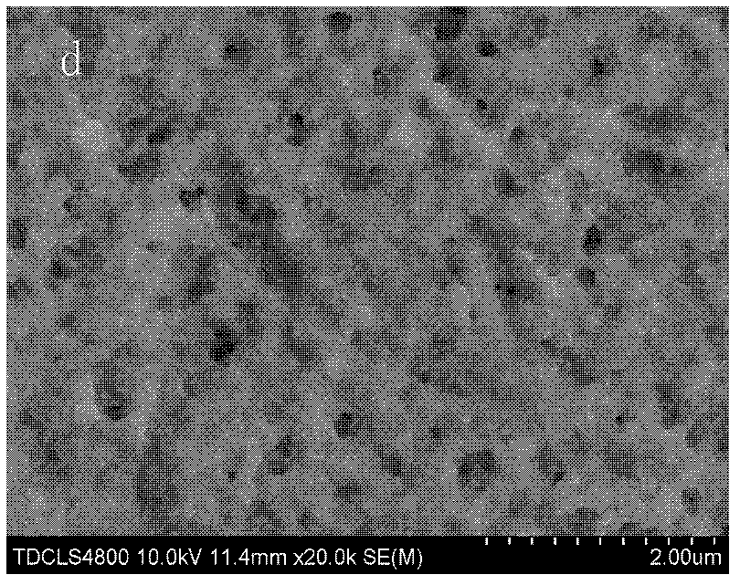
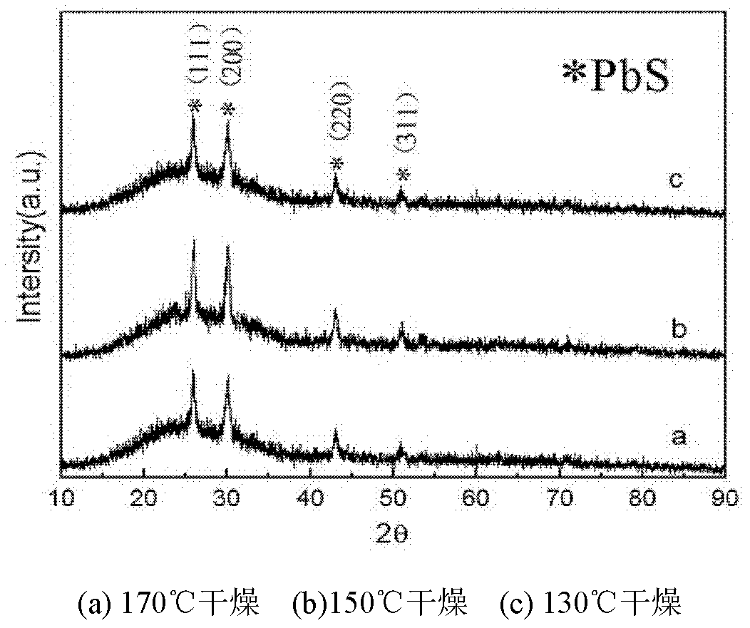
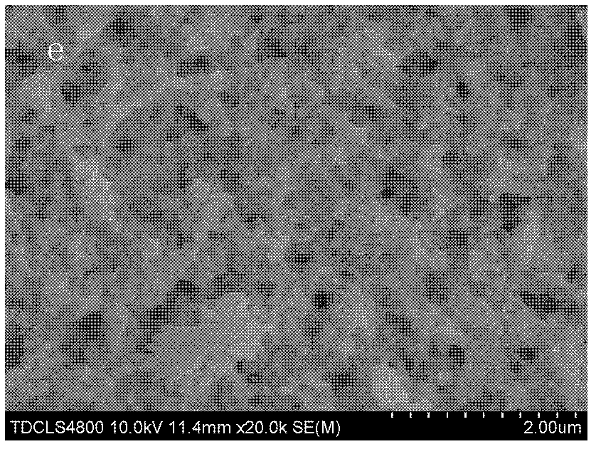
[0025] The raw materials used in the present invention are all commercially available raw materials whose purity is analytically pure. Figure 17 It is a process flow diagram of the in-situ chemical reaction method for the preparation of PbS thin films, and specific examples are shown in Table 1.
[0026] Table 1
[0027]
Login to View More PUM
 Abstract
The invention discloses a method for synthesizing a lead sulfide (PbS) film through the chemical in-situ reaction of a solution. The method comprises the steps of: (1) preparing a precursor solution; (2) preparing the PbS film through carrying out an in-situ reaction: vertically immerging a deposition substrate, of which a lead precursor film is attached to the surface, into a sulfur source anionic precursor solution for carrying out an in-situ chemical reaction, after 10 seconds, pulling the deposition substrate out of the reaction solution at a uniform speed, washing the deposition substrate by using deionized water, then, placing the deposition substrate in a drying box so as to form a PbS reaction deposition layer; and (3) carrying out heat treatment. The invention provides a novel in-situ chemical synthesizing method for the PbS film with high efficiency, convenience, little pollution and low cost, low-toxicity chemical raw materials, such as inorganic salt which serves as a precursor, alcohol ether and alcohol amine which serve as solvents, and the like, are adopted, and the PbS film is synthesized at a lower temperature, so that method for synthesizing the PbS film through the chemical in-situ reaction of the solution has the advantages of good evenness in solution deposition reaction, high degree of crystallizing, and easiness for controlling the thickness of the film.
Description
Technical field [0001] The present invention relates to the synthesis of lead sulfide films, and in particular to a method for synthesizing lead sulfide films by in-situ reaction of solution chemical. Background technique [0002] Lead sulfide (PbS) has a NaCl crystal structure and is an important group IV-VI semiconductor. It has a narrow direct band gap energy (0.41eV, 300K) and a large exciton Bohr radius (18nm). Engineering technology has been widely used. [0003] The monodisperse, nanoscale structure of semiconductor crystals has a quantum confinement effect and exhibits unique optical and electrical properties due to its at least one-dimensional scale in the nanoscale. Nanostructured PbS has a strong quantum confinement effect. Its nanoparticles are close to the absorption boundary of the solar cell due to the blue shift. The electronic energy band spans the infrared spectral region from 900 to 1600 nm. A fluorescence emission peak appears at 1641 nm in the near-infrared re...
Claims
Login to View More Application Information
Patent Timeline
 IPC IPC(8): C01G21/21C03C17/22
Inventor靳正国王鑫
OwnerTIANJIN UNIV