Transfer plate with metal vertical interconnection structure and manufacture method thereof
A technology of vertical interconnection and manufacturing method, applied in the field of three-dimensional stacking, can solve the problems of complex process and high cost of manufacturing three-dimensional stacked chips, and achieve the effects of simplified process steps, simple structure and convenient operation.
- Summary
- Abstract
- Description
- Claims
- Application Information
AI Technical Summary
Problems solved by technology
Method used
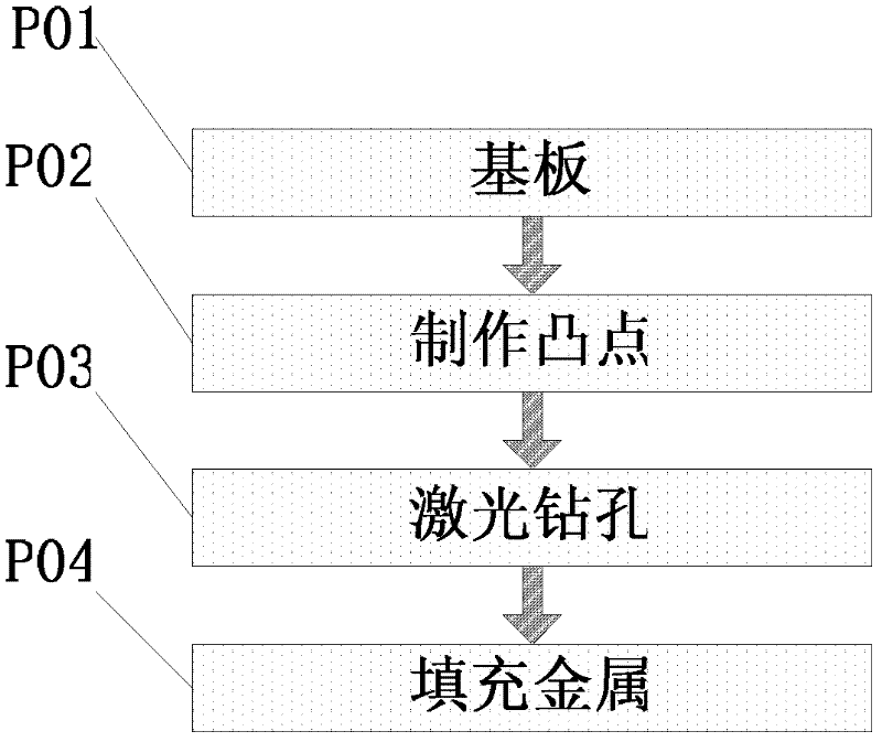
Image

Examples
Embodiment 1
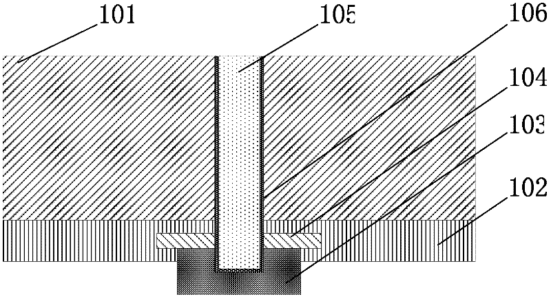
[0044] First, refer to figure 1 Embodiment 1 of the metal vertical interconnection structure applied to three-dimensional stacked chips disclosed in the present invention will be introduced. This Embodiment 1 is a specific structure when the present invention is applied to an interposer.
[0045] in such as figure 1 The shown interposer structure includes a substrate 101 . In this embodiment, the material of the substrate 101 is glass, but it may also be silicon or organic material. There is a passivation layer 102 on the lower surface of the substrate 101 . The material of the passivation layer 102 is polyimide in this embodiment. There is a metal bump structure on the lower surface side of the passivation layer 102, the metal bump structure includes a pad 104, which is buried inside the passivation layer 102, and a metal bump 103 is arranged on the lower surface of the pad 104 . In this embodiment, the pad 104 is made of metal aluminum. In this embodiment, the materia...
Embodiment 2
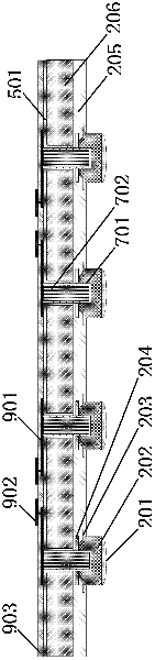
[0055] image 3 A metal vertical interconnection structure applied to three-dimensional stacked chips according to Embodiment 2 of the present invention is depicted. Specifically, this second embodiment is also a specific structure when the present invention is applied to an interposer.
[0056] in such as image 3 In the illustrated interposer, a substrate 206 is included. In Example 2, the substrate 206 is a 4-inch silicon wafer with a thickness of 200 microns. Optionally, the material of the substrate 206 may also be glass or organic material. On the lower surface of the substrate 206 there is a passivation layer 205 . There is a metal bump structure in the passivation layer 205 , a part of the metal bump structure is embedded in the passivation layer 205 , and another part protrudes from the lower surface of the passivation layer 205 .
[0057] Specifically, the metal bump structure includes pads 204 , underlying metal layer 203 , metal pillars 202 and solder 201 . W...
PUM
| Property | Measurement | Unit |
|---|---|---|
| Thickness | aaaaa | aaaaa |
| Thickness | aaaaa | aaaaa |
| Thickness | aaaaa | aaaaa |
Abstract
Description
Claims
Application Information
PatSnap Eureka turns technology decisions into work you can execute. Powered by our Innovation Knowledge Graph, it runs expert workflows across engineering, life sciences, materials and intellectual property. Get your review-ready output in minutes.


