CMOS (Complementary Metal-Oxide-Semiconductor Transistor) for inhibiting drain induced barrier lowering effect and manufacturing method of CMOS

A technology of sensing barriers and MOS transistors, applied in the field of CMOS devices, to achieve the effects of suppressing DIBL effect, low implementation cost, and improving performance

Active Publication Date: 2012-04-18
SHANGHAI HUALI MICROELECTRONICS CORP
View PDF5 Cites 3 Cited by
  • Summary
  • Abstract
  • Description
  • Claims
  • Application Information

AI Technical Summary

Problems solved by technology

[0006] The invention provides a method for suppressing the induced barrier lowering effect of the semiconductor drain, aiming at the existing deficiencies in suppressing the DIBL effect, by implanting ions into the semiconductor gate close to the drain to locally change the work function of the gate, thereby achieving suppression The purpose of the DIBL effect will not cause an additional increase in the leakage current of the PN junction at the drain

Method used


Image

  • CMOS (Complementary Metal-Oxide-Semiconductor Transistor) for inhibiting drain induced barrier lowering effect and manufacturing method of CMOS
  • CMOS (Complementary Metal-Oxide-Semiconductor Transistor) for inhibiting drain induced barrier lowering effect and manufacturing method of CMOS
  • CMOS (Complementary Metal-Oxide-Semiconductor Transistor) for inhibiting drain induced barrier lowering effect and manufacturing method of CMOS

Examples


Embodiment 1

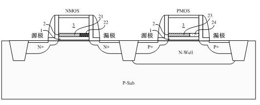
[0061] Such as figure 1 As shown, the gates of the N-type MOS transistor and the P-type MOS transistor of the CMOS device of the present invention all include a high dielectric layer 1, a metal oxide dielectric material layer 2 and a layer of polysilicon or metal layer 3 , and the metal oxide dielectric material layer 2 near the drain contains ions that change the work function of the metal oxide dielectric material layer 2 implanted near the drain end, and the work function of the metal oxide dielectric material The function is changed, so that the work function of the metal oxide dielectric material layer 2 near the source end and the drain end are different.

[0062] Wherein, in the metal oxide dielectric material layer 2 of the N-type MOS transistor gate, the ions are ions with a large work function, which effectively increases the metal oxide dielectric material layer 2, The work function near the drain end portion 22 makes the work function of the metal oxide dielectric...

Embodiment 2

[0074] And the following embodiments 2 and 3 are the same)

[0075]Step 4. Deposit a layer of polysilicon or metal layer 3 on the metal oxide dielectric material layer 2, for polysilicon or metal layer 3, thin oxide layer of N or PMOS, high dielectric layer 1 and metal oxide dielectric material Layer 2 is etched, and only part of the polysilicon or metal layer 3, the thin oxide layer of N or PMOS, the high dielectric layer 1 and the metal oxide dielectric material layer 2 for preparing the respective gates of NMOS and PMOS are reserved, Respectively form gates of NMOS and PMOS;

[0076] Step 5. Perform ion implantation in the drain-source regions of NMOS and PMOS, wherein, the drain electrode of NMOS near the first ion implantation region in the ion implantation region of NMOS; the drain electrode of NMOS near the second ion implantation region in the ion implantation region of PMOS is Drain of the PMOS.
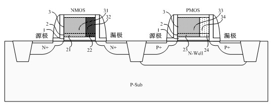
[0077] Example 2:

[0078] Such as figure 2 As shown, in this embo...

Embodiment 3

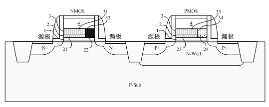
[0092] Such as image 3 As shown, in this embodiment, the metal oxide dielectric material layer 2 is covered with two polysilicon or metal layers, the first polysilicon or metal layer 3 and the second polysilicon or metal layer 4, wherein the The second polysilicon or metal layer 4 covers the first polysilicon or metal layer 3, and only the first polysilicon or metal layer 3 is implanted with ions of different work functions near the drain terminal. . Moreover, in this embodiment, for the entire polysilicon or metal layer (polysilicon or metal layer 3 and polysilicon or metal layer 4 ), work function adjustment is performed on half polysilicon or metal layer (Half Poly or Metal).

[0093] The difference between this embodiment and Embodiment 2 is that this embodiment includes two polysilicon or metal layers, a first polysilicon or metal layer 3 and a second polysilicon or metal layer 4 . The first polysilicon or metal layer 3 is implanted with ions that change the work funct...


PUM


Abstract

The invention provides a CMOS (Complementary Metal-Oxide-Semiconductor Transistor) for inhibiting a drain induced barrier lowering effect and a manufacturing method of the CMOS. The CMOS comprises an N-type MOS (Metal-Oxide-Semiconductor) transistor and a P-type MOS transistor, wherein a gate of the N-type MOS transistor and a gate of the P-type MOS transistor respectively comprise a high dielectric layer, a metal oxide dielectric material layer and polysilicon or a metal layer; and ions with different work functions are implanted in the metal oxide dielectric material layer and the polysilicon or the metal layer, so that a work function of the gate of the N-type MOS transistor, which is close to the drain electrode end, is increased, a work function of the gate of the P-type MOS transistor, which is close to the drain electrode end, is reduced and further the drain induced barrier lowering effect of the CMOS is inhibited. While the DIBL (Drain Induced Barrier Lowering) effect is effectively inhibited by changing the work function of the gate of the CMOS, which is close to the drain electrode end, extra increase of drain end PN (Peripheral Node) leakage current can be avoided and the performance of a semiconductor chip is effectively improved; in addition, the manufacturing method has the advantages of simple process flow, low implementation cost and avoidance of extra cost burden.

Description

technical field [0001] The invention relates to a method for manufacturing an integrated circuit, in particular to a CMOS device that suppresses the effect of reducing the drain induction potential barrier. Background technique [0002] Drain induction barrier lower (DIBL) effect is an undesirable phenomenon that occurs in small-sized field effect transistors (FETs) in the semiconductor manufacturing process, that is, when the channel length is reduced, the drain region source The interval voltage (Vds) increases, so that when the depletion layer of the drain junction and the source junction is close, the electric force line in the channel can cross from the drain region to the source region, and cause the barrier height of the source terminal to decrease, so that the source region is injected into the channel The number of electrons increases, resulting in an increase in the drain current. And when the channel length is shorter, the DIBL effect is more serious. [0003] T...

Claims


Application Information

Patent Timeline
Patent Type & Authority Applications(China)
IPC IPC(8): H01L27/092H01L29/78H01L29/51H01L21/8238
Inventor 黄晓橹谢欣云陈玉文邱慈云
Owner SHANGHAI HUALI MICROELECTRONICS CORP
Why Eureka
Try Eureka