Back scattering surface of thin-film silicon solar cell and preparation method of back scattering surface

A solar cell and backscattering technology, which is applied in circuits, photovoltaic power generation, electrical components, etc., can solve problems such as difficulty in realization, and achieve the effects of reducing production costs, improving optical and electrical properties, and simplifying processes

Inactive Publication Date: 2012-04-18
TONGJI UNIV
View PDF4 Cites 1 Cited by
  • Summary
  • Abstract
  • Description
  • Claims
  • Application Information

AI Technical Summary

Problems solved by technology

However, the existing metallic Ag film backscattering surface is obtained by depositing Ag film on the substrate first, and then heating the film in a high vacuum chamber. In order to form a rough structure

Method used


Image

  • Back scattering surface of thin-film silicon solar cell and preparation method of back scattering surface
  • Back scattering surface of thin-film silicon solar cell and preparation method of back scattering surface
  • Back scattering surface of thin-film silicon solar cell and preparation method of back scattering surface

Examples


Embodiment 1

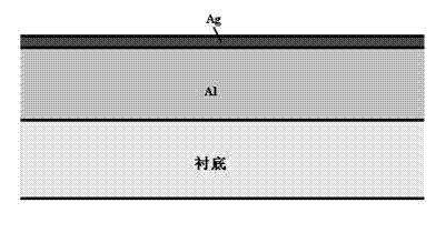
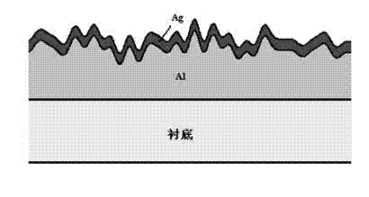
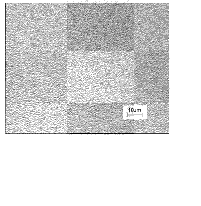
[0040] Using the physical vapor deposition method (double-boat dual-source evaporation process), in a high-vacuum environment: under the condition of heating the glass substrate to 250°C, first deposit an Al film with a thickness of 400 nm on the substrate, and then deposit a thickness of The Ag film at 20 nm constitutes an Al / Ag composite film, that is, a roughened backscattering surface. Such as image 3 As shown, it can be seen that the surface of the film presents a submicron-scale structural morphology.

Embodiment 2

[0042] Using the physical vapor deposition method (double-boat dual-source evaporation process), in a high vacuum environment: at room temperature, an Al film with a thickness of 400 nm is deposited on a glass substrate, and then an Ag film with a thickness of 50 nm is deposited. The Al / Ag composite film is formed, and then the deposited composite film is subjected to vacuum heat treatment at 250° C. to make a roughened back-scattering surface. Such as Figure 4 As shown, it can be seen that the surface of the film presents a submicron-scale structural morphology.

Embodiment 3

[0044] Using the physical vapor deposition method (double-boat dual-source evaporation process), in a high-vacuum environment: under the condition of heating the glass substrate to 150°C, first deposit a Sn film with a thickness of 400 nm on the substrate, and then deposit a thickness of The Ag film at 30 nm constitutes a Sn / Ag composite film, that is, a back-scattering surface with roughened surface. Such as Figure 5 As shown, it can be seen that the surface of the film presents a micron-scale structural morphology.


PUM


Abstract

The invention relates to a back scattering surface of a thin-film silicon solar cell and a preparation method of the back scattering surface. In the invention, a thin film which is used as the back scattering surface is a composite film and is compounded by a metal and an Ag film, wherein the metal is in direct contact with a substrate and has a shape which is easy to change at a lower temperature; the thickness of the metal film is in a range of 250-600 nm and the thickness of the Ag film is in a range of 20-50 nm; and the surface of the composite film is of a rough structure shape with a submicron size. The structure is prepared by adopting a physical vapor deposition method; in a high-vacuum environment, the method comprises the following steps of: under the condition of heating the substrate, depositing the metal film on the substrate and then depositing the Ag film to form the composite film; or under the condition of the room temperature, depositing the metal film on the substrate and then depositing the Ag film to form the composite film; and then carrying out vacuum heat treatment on the deposited composite film at a temperature in a range of 150-250 DEG C. According to the invention, the scattering property of the surface of the formed composite film is great, the temperature for changing the shape of the metal film is lower and the heat treatment temperature for reducing surface roughening is reduced; meanwhile, the consumption of the noble metal Ag is reduced and the manufacturing cost is reduced.

Description

technical field [0001] The technology of the invention relates to material science, green energy, and physical optics, and has application prospects in the research field of solar thin film batteries. Background technique [0002] Under the situation of shortage of conventional energy and environmental pollution, leading to global warming and deterioration of the human ecological environment, the development and utilization of new energy in line with the sustainable development strategy has attracted more and more attention from all over the world. Photovoltaic energy has become the most important new energy in the 21st century because of its advantages that other conventional energy sources do not have, such as sufficient cleanliness, absolute safety, relative breadth and adequacy of resources, long life, and maintenance-free. One of energy. [0003] A solar photovoltaic cell is a semiconductor device that converts light energy into electrical energy. Crystalline silicon ...

Claims


Application Information

Patent Timeline
IPC IPC(8): H01L31/0216H01L31/0236H01L31/18
CPCY02E10/50Y02P70/50
Inventor 吴永刚刘仁臣夏子奂唐平林
Owner TONGJI UNIV
Why Eureka
Try Eureka