Preparation method of wide-spectrum and strong-absorption surface-photovoltage type photodetector

A photodetector and photovoltaic technology, which is applied in semiconductor devices, final product manufacturing, sustainable manufacturing/processing, etc., can solve problems such as limited spectral range, complex structure, and limited application range, and achieve broad application prospects and low production costs. Low, wide spectral range effects

Inactive Publication Date: 2012-04-25
SOUTHWEST JIAOTONG UNIV
View PDF4 Cites 7 Cited by
  • Summary
  • Abstract
  • Description
  • Claims
  • Application Information

AI Technical Summary

Problems solved by technology

However, the applicable spectral range of these detectors is limited, and the spectral response range is fixed and cannot be adjusted, which limits its application range
If it is used for spectral analysis and calibration, it is necessary to use many photodetectors in various spectral bands at the same time, resulting in complex structure and troublesome operation
Although silicon photodetectors are suitable for a wide spectral range, their preparation usually requires complex energy-intensive production processes such as smelting, crystallization, and segmentation, making them expensive to use, and silicon detectors do not have adjustable spectral response ranges. characteristic

Method used


Image

  • Preparation method of wide-spectrum and strong-absorption surface-photovoltage type photodetector
  • Preparation method of wide-spectrum and strong-absorption surface-photovoltage type photodetector
  • Preparation method of wide-spectrum and strong-absorption surface-photovoltage type photodetector

Examples


specific Embodiment approach

[0029] A specific embodiment of the present invention is: a preparation method of a broad-spectrum, strong-absorbing surface photovoltaic photodetector, the specific method of which is:

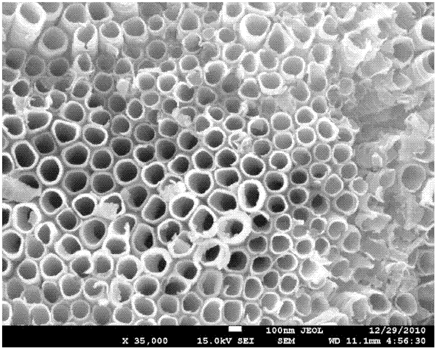
[0030] a. TiO 2 Fabrication and Crystallization of Nanotube Arrays

[0031] With titanium foil as anode, platinum as cathode, 0.25wt% NH 4 The ethylene glycol solution of F is the electrolyte, and the titanium foil is anodized for 3 hours; the titanium foil is taken out, rinsed with deionized water, and ultrasonically treated for 5 minutes to obtain amorphous TiO on the titanium foil. 2 nanotube arrays;

[0032] Titanium foil and its amorphous TiO 2 The nanotube array was heated up to 450°C at a rate of 3°C / min, held for 3 hours and annealed for 3 hours, and finally cooled to room temperature with the furnace, that is, anatase TiO was formed on the titanium foil immersed in the electrolyte. 2 Nanotube array, no product attached to the part of the titanium foil that is not immersed in the ...

Embodiment 2

[0046] The specific approach in this example is

[0047] a. TiO 2 Fabrication and Crystallization of Nanotube Arrays

[0048] With titanium foil as anode, platinum as cathode, 0.25wt% NH 4 The ethylene glycol solution of F is the electrolyte, and the titanium foil is anodized for 6 hours; the titanium foil is taken out, rinsed with deionized water, and ultrasonically treated for 8 minutes to obtain amorphous TiO on the titanium foil. 2 nanotube arrays;

[0049] Titanium foil and its amorphous TiO 2 The nanotube array is heated up to 450°C at a rate of 20°C / min, held for 3.5 hours, and finally cooled to room temperature with the furnace, that is, anatase TiO is formed on the titanium foil immersed in the electrolyte. 2 Nanotube array, no product attached to the part of the titanium foil that is not immersed in the electrolyte;

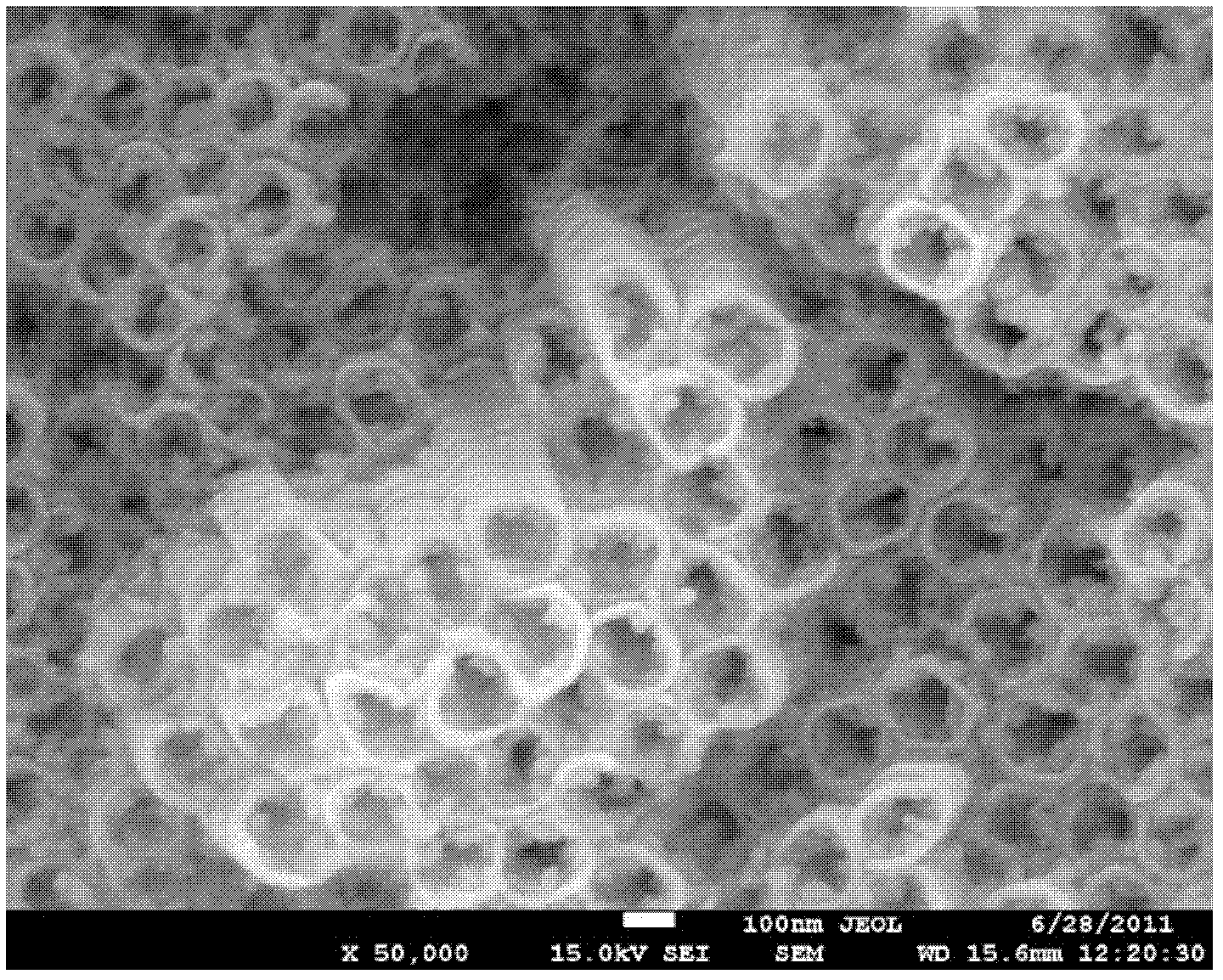
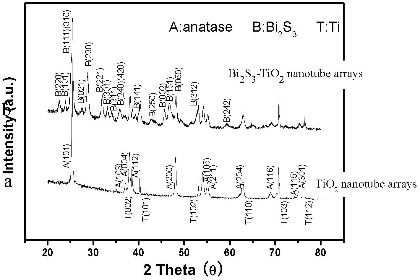
[0050] b. Preparation of Bi by hydrothermal method 2 S 3 -TiO 2 nanotube array

[0051] Na 2 S 2 o 3 Added to 0.008mol / L Bi(NO 3 ) 3 The ...

Embodiment 3

[0058] The specific approach in this example is

[0059] a. TiO 2 Fabrication and Crystallization of Nanotube Arrays

[0060] With titanium foil as anode, platinum as cathode, 0.25wt% NH 4 The ethylene glycol solution of F is the electrolyte, and the titanium foil is anodized for 5 hours; the titanium foil is taken out, rinsed with deionized water, and ultrasonically treated for 6 minutes to obtain amorphous TiO on the titanium foil. 2 nanotube arrays;

[0061] Titanium foil and its amorphous TiO 2 The nanotube array was heated to 450°C at a rate of 10°C / min, held for 4 hours, and finally cooled to room temperature with the furnace, that is, anatase TiO was formed on the titanium foil immersed in the electrolyte. 2 Nanotube array, no product attached to the part of the titanium foil that is not immersed in the electrolyte;

[0062] b. Preparation of Bi by hydrothermal method 2 S 3 -TiO 2 nanotube array

[0063] Na 2 S 2 o 3 Added to 0.009mol / L Bi(NO 3 )3 The react...


PUM

PropertyMeasurementUnit
sizeaaaaaaaaaa

Abstract

The invention relates to a preparation method of a wide-spectrum and strong-absorption surface-photovoltage type photodetector, comprising the following steps of: adopting a titanium foil as a positive electrode, adopting platinum as a negative electrode, carrying out oxidation on the titanium foil and obtaining an amorphous TiO2 nano tube array; after treatment, obtaining a TiO2 nano tube array;putting the titanium foil in a high-temperature reaction kettle, then injecting aqueous solution of Na2S2O3 and Bi(NO3)3 into the sealed reaction kettle, carrying out heat treatment and obtaining a Bi2S3-TiO2 nano tube array; covering FTO on the surface of the Bi2S3-TiO2 nano tube array, leading out an electrode; leading out an electrode on the titanium foil without generating the Bi2S3-TiO2 nanotube array; and packaging the contact edges of the FTO, the titanium foil and the Bi2S3-TiO2 nano tube array to obtain the photodetector. The method is low in energy consumption and simple in processand equipment; and the prepared photodetector is applicable to a large spectrum range, is suitable for spectrum analysis, can also be used as photoelectric devices such as a photosensitive switch andthe like and has wide application prospect.

Description

technical field [0001] The invention relates to a preparation method of a surface photovoltaic photodetector with broad spectrum and strong absorption. Background technique [0002] Photodetectors are sensors made of materials with photoelectric effects that can realize photoelectric conversion, and their function is to realize photoelectric conversion. The mechanism is that the guided beam injected into the detector causes the stimulated transition of electrons from the valence band to the conduction band to generate photogenerated carriers (electrons and holes). And these carriers are collected by the PN junction or Schottky barrier, and finally manifested as photovoltage or photocurrent. Due to the specific band gap of photoelectric materials, most photodetectors have strong spectral selectivity, that is, the spectral responsivity of different photodetectors is different at different wavelengths. Such as deep ultraviolet detectors responding to solar blind areas, solar ...

Claims


Application Information

Patent Timeline
Patent Type & Authority Applications(China)
IPC IPC(8): H01L31/18
CPCY02P70/50
Inventor 杨峰蔡芳共赵勇
Owner SOUTHWEST JIAOTONG UNIV
Why Eureka
Try Eureka