Method for increasing metal-insulating layer-metal (MIM) capacitor density in semiconductor device and structure thereof

A semiconductor and device technology, applied in the field of capacitor structure and its manufacturing, can solve the problems of not being able to improve the capacitance density and increase the manufacturing cost, and achieve the effect of increasing the capacitance density and strong compatibility

Active Publication Date: 2012-05-02
SHANGHAI HUALI MICROELECTRONICS CORP
View PDF5 Cites 6 Cited by
  • Summary
  • Abstract
  • Description
  • Claims
  • Application Information

AI Technical Summary

Problems solved by technology

[0008] The purpose of the present invention is to solve the defect that the capacitance density cannot be i

Method used


Image

  • Method for increasing metal-insulating layer-metal (MIM) capacitor density in semiconductor device and structure thereof
  • Method for increasing metal-insulating layer-metal (MIM) capacitor density in semiconductor device and structure thereof
  • Method for increasing metal-insulating layer-metal (MIM) capacitor density in semiconductor device and structure thereof

Examples


Embodiment Construction

[0073] The present invention will be described in further detail below in conjunction with the accompanying drawings and specific embodiments. The specific embodiments described here are only used to explain the present invention, and are not used to limit the protection scope of the present invention.

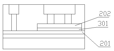
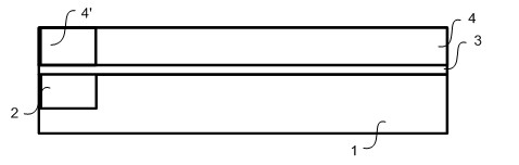
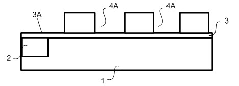
[0074] Reference in turn Figure 2 to Figure 9 Shown is a schematic diagram of the structure when multiple steps of the method according to the present invention are executed. in, Figure 9 The block diagram shown is a semiconductor device containing high-density MIM (metal-insulator-metal) capacitors.

[0075] Such as figure 2 As shown, in one embodiment, in a method for increasing the capacitance density of MIM (metal-insulator-metal) in a semiconductor device provided by the present invention, the insulating substrate 1 is usually used as a certain interlayer dielectric in the semiconductor device Layer (ILD), in the insulating substrate 1 is usually provided with meta...


PUM

PropertyMeasurementUnit
Thicknessaaaaaaaaaa
Thicknessaaaaaaaaaa

Abstract

The invention discloses a method for increasing the metal-insulating layer-metal (MIM) capacitor density in a semiconductor device and the semiconductor device comprising a high-density MIM capacitor. An appearance layer is arranged on a blocking layer of a base, the appearance layer is etched so that the appearance layer is provided with a plurality of grooves, and a capacitor base plate covered on the appearance layer is in an appearance shape for increasing the area of the capacitor base plate, so the capacitor density is increased, and simultaneously, the matching of a high capacitor and a copper metal electrode plate is realized through the appearance layer. Compared with the prior art, the method and the semiconductor device have the advantages that the wafer area is not increased, and simultaneously, the method has high compatibility with the traditional process.

Description

technical field [0001] The invention relates to the capacitor structure included in an integrated circuit and the field of manufacture thereof, in particular to a method for increasing the capacitance density of an MIM in a semiconductor device and its structure. Background technique [0002] The continuous innovation of semiconductor integrated circuit manufacturing process technology has made the integration level higher and higher. While realizing as many devices as possible in the smallest possible area, it is also required to obtain the highest possible performance. [0003] Among them, capacitors are an important component unit in integrated circuits, and are widely used in chips such as memory, microwave, radio frequency, smart card, high voltage and filtering. With the reduction of chip size and the high demand for large capacitance performance, how to obtain high-density capacitance in a limited area has become a very attractive topic. [0004] The traditional capa...

Claims


Application Information

Patent Timeline
IPC IPC(8): H01L21/02H01L23/522
Inventor 胡友存张亮姬峰李磊陈玉文
Owner SHANGHAI HUALI MICROELECTRONICS CORP
Why Eureka
Try Eureka