Patterned substrate for controlling gallium nitride nucleating growth position and preparation method thereof

A graphic substrate, gallium nitride technology, applied in electrical components, circuits, semiconductor devices, etc., can solve problems such as epitaxial growth defects of LED chips, and achieve the effects of reducing crystal defects, improving chip brightness, and improving crystal quality.

Active Publication Date: 2012-05-02
EPILIGHT TECH
View PDF4 Cites 10 Cited by
  • Summary
  • Abstract
  • Description
  • Claims
  • Application Information

AI Technical Summary

Problems solved by technology

[0006] In view of the shortcomings of the prior art described above, the purpose of the present invention is to provide a pattern substrate for controlling the nucleation positio

Method used


Image

  • Patterned substrate for controlling gallium nitride nucleating growth position and preparation method thereof
  • Patterned substrate for controlling gallium nitride nucleating growth position and preparation method thereof
  • Patterned substrate for controlling gallium nitride nucleating growth position and preparation method thereof

Examples


Embodiment 1

[0027] see Figure 2 to Figure 5 , as shown in the figure, the present invention provides a method for preparing a graphics substrate for controlling the nucleation position of gallium nitride growth, and the method at least includes the following steps:

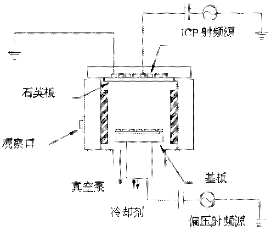
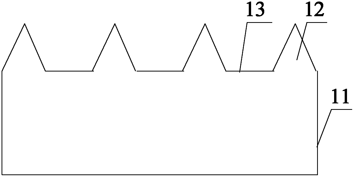
[0028] see figure 2 , as shown in the figure, at first step 1) is performed, a semiconductor substrate 11 is provided, and the semiconductor substrate 11 is etched for the first time to form a plurality of raised microstructures 12 on its surface, and each raised There are gap platforms 13 between the microstructures. In this embodiment, the semiconductor substrate 11 is a sapphire substrate, and the first etching is carried out in ICP etching equipment. In the specific implementation process, the surface is made of periodically arranged photoresist The patterned sapphire substrate is loaded into the ICP etching equipment, using BCl 3 gas as etchant gas or BCl 3 and Cl 2 The mixed gas is used as the etching gas, and th...

Embodiment 2

[0033] see Figure 2 to Figure 5 , as shown in the figure, the basic implementation steps of the preparation method of the graphic substrate used to control the growth and nucleation position of gallium nitride are as in Example 1, and in the dry etching equipment, the power of the RF radio frequency source is Between 30% and 50% of the rated power, the power of the bias RF source is 50% to 80% of the rated power of the equipment, the etching pressure is 0.2 to 0.5pa, the gas flow is 50 to 150sccm, and the processing time is 5 to 10 minutes .

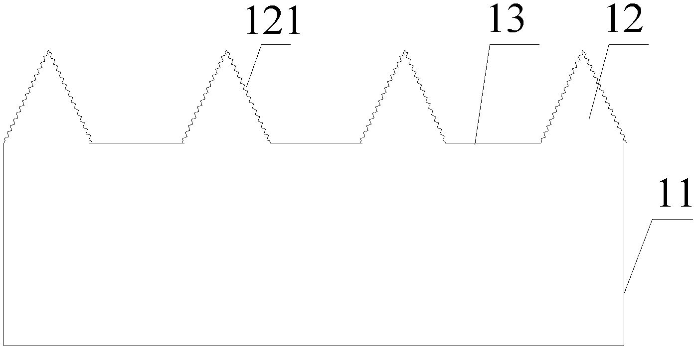
[0034] see image 3 , as shown in the figure, the structure of the graphics substrate used to control the growth and nucleation position of GaN is as shown in Embodiment 1.

[0035] Through the processing technology of the invention, a high-quality patterned sapphire substrate can be produced, and the light extraction efficiency of the LED chip can be improved. After graphic surface treatment, the brightness can be increased by 10%, ...


PUM


Abstract

The invention provides a patterned substrate for controlling a gallium nitride nucleating growth position and a preparation method thereof. The method comprises the following steps that: the first-time etching is performed on a sapphire substrate, convex micro structures and clerance platforms which are periodically arranged are formed on the surface of the sapphire substrate, then fluoride ion is used for treating the surface of the patterned substrate on the basis of the characteristics that the sapphire has different physical properties and chemical properties in different crystallographic orientations, the surface of the convex micro structure in the fluoride ion is corroded into a coarse surface, the clearance platform between every two adjacent convex micro structures is not influenced, when extension of the patterned substrate after the surface treatment is grown, the convex micro structure surface is corroded into the coarse surface, no growth platform exists during the extension growth process, the nucleation cannot be formed; and since a large platform is arranged between the convex micro structures, a gap between the convex micro structures can be promoted to nucleat in the vertical direction. By adopting the extension layer which is grown in the above way, the flaw of the crystal is obviously reduced, the crystal quality can be improved, and the brightness of a chip can be improved.

Description

technical field [0001] The invention belongs to the field of semiconductors, in particular to a pattern substrate for controlling the growth and nucleation position of gallium nitride and a preparation method thereof. Background technique [0002] Light-emitting diodes have the advantages of small size, high efficiency and long life, and are widely used in traffic indication, outdoor full-color display and other fields. In particular, the use of high-power light-emitting diodes may realize semiconductor solid-state lighting, which has caused a revolution in the history of human lighting, and has gradually become a research hotspot in the field of electronics. In order to obtain high-brightness LEDs, the key is to improve the internal quantum efficiency and external quantum efficiency of the device. At present, the light extraction efficiency of the chip is the main factor limiting the external quantum efficiency of the device. The main reason is that the refractive index di...

Claims


Application Information

Patent Timeline
IPC IPC(8): H01L33/00H01L33/22
Inventor 袁根如郝茂盛李士涛张楠朱广敏陈诚邢志刚陈耀汪洋李睿彭昀鹏
Owner EPILIGHT TECH
Why Eureka
Try Eureka