Dual complementary metal oxide semiconductor (CMOS) image sensor pixel unit with high filling factor, and working method

An image sensor, pixel unit technology, applied in image communication, TV system components, electrical components, etc., can solve the problems of sensitivity, signal-to-noise ratio fill factor degradation, etc., achieve convenient control, reduce off-state leakage current, structure simple effect

Active Publication Date: 2012-05-09
PKU HKUST SHENZHEN HONGKONG INSTITUTION
View PDF3 Cites 5 Cited by
  • Summary
  • Abstract
  • Description
  • Claims
  • Application Information

AI Technical Summary

Problems solved by technology

With the increase of integration density and complexity of today's integrated circuits, reducing the pixel unit size has become the main driving force for the development and competition of CIS, but the degradation of sensitivity, signal-to-noise ratio, fill factor, etc. Here comes the big challenge

Method used


Image

  • Dual complementary metal oxide semiconductor (CMOS) image sensor pixel unit with high filling factor, and working method
  • Dual complementary metal oxide semiconductor (CMOS) image sensor pixel unit with high filling factor, and working method
  • Dual complementary metal oxide semiconductor (CMOS) image sensor pixel unit with high filling factor, and working method

Examples


Embodiment 1

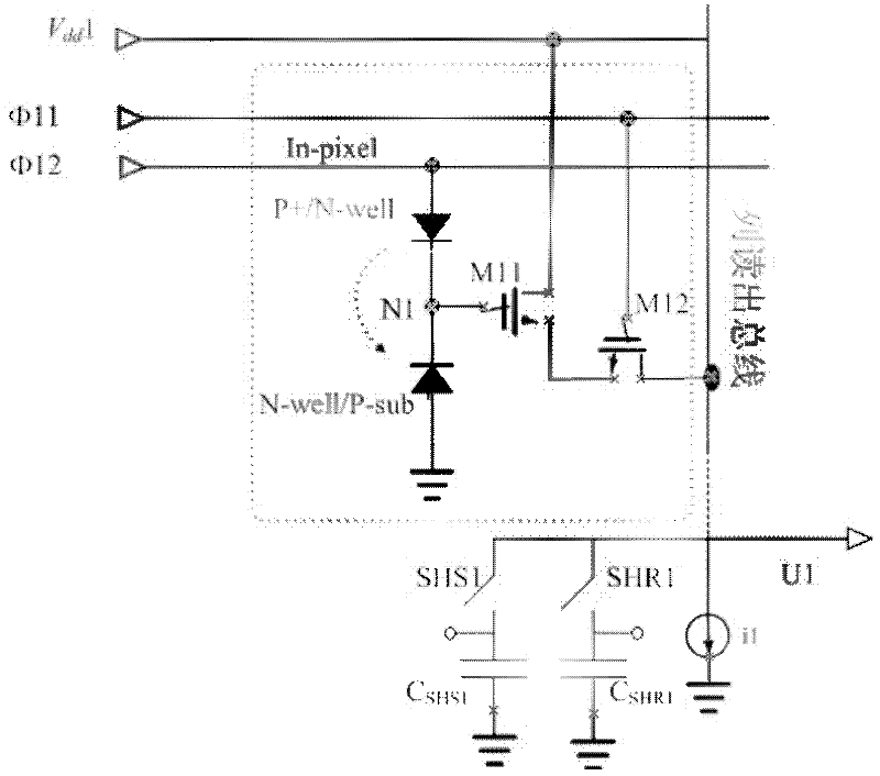
[0038] The AMIS (ON Semiconductor) CMOS technology and rules with a thickness of 0.35um are adopted, so that each pixel unit only needs a 2T-APS test structure with one polysilicon layer and five metal layers, and each pixel unit size is 7um×7um.

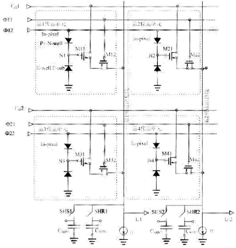
[0039] The chip of this embodiment specifically adopts the simplest 2T-APS pixel array of 2×2 pixel units, and its equivalent circuit is as follows figure 2 As shown, the corresponding layout is as Figure 4 shown.

[0040] The circuit structure of each pixel unit of the pixel array chip, the equivalent circuit is as figure 1 As shown, wherein: N1 is a diode with a P+ / N-Well / P-sub structure, and its P+ terminal is electrically connected to the reset control signal Φ11; M11 is a source follower transistor, and its base is electrically connected to the P+ / N- Diode N1 of Well / P-sub structure, the collector is electrically connected to the bias voltage Vdd1; M12 is a selection transistor, the emitter is electrically connected to the ...


PUM


Abstract

The invention relates to a dual complementary metal oxide semiconductor (CMOS) image sensor pixel unit with a high filling factor, and a working method. The pixel unit only comprises a diode (N1) with a P+/N-Well/P-sub structure, a source following transistor (M11) and a selecting transistor (M12). The corresponding pixel array working method comprises the following steps of: resetting, namely applying a selecting control signal (phi12) with high positive voltage and a resetting control signal (phi11) with high positive voltage to activate the diode (N1) with the P+/N-Well/P-sub structure to charge a node; optically-integrating, namely setting the phi12 and the phi11 to be low positive voltage within a fixed illumination integration time period, wherein a current carrier is produced by partial accumulated light of the N-Well/P-sub structure in the diode, and the node is discharged; and reading out, namely after light integration, changing the phi12 to be the high positive voltage, and reading a light sensing signal corresponding to the current carrier out by column buses through the M11 and the M12.

Description

technical field [0001] The invention relates to the technical field of integrated circuits, in particular to a pixel unit of a dual complementary metal oxide semiconductor (CMOS) image sensor with a high filling factor and a working method thereof. Background technique [0002] Image sensing technology has penetrated into the life of modern people, such as: photography, photography and so on. The CMOS image sensor (CIS) has gradually replaced the charge-coupled device (CCD) image sensor based on its own advantages of low cost, low power consumption, and high integration capability. The characteristics of CIS are mainly determined by resolution, fill factor, dark current, temporal noise, fixed pattern noise, sensitivity, responsivity, quantum efficiency, dynamic range, and signal-to-noise ratio. With the increase of integration density and complexity of today's integrated circuits, reducing the pixel unit size has become the main driving force for the development and competi...

Claims


Application Information

Patent Timeline
Patent Type & Authority Applications(China)
IPC IPC(8): H04N5/374H01L27/146
Inventor 何进苏艳梅张东维
Owner PKU HKUST SHENZHEN HONGKONG INSTITUTION
Why Eureka
Try Eureka