

Novel organic electroluminescent compounds and organic electroluminescent device using the same
A technology of luminescence and compounds, applied in the field of organic electroluminescent devices, can solve the problems of reduced quantum yield and reduced device operating life
- Summary
- Abstract
- Description
- Claims
- Application Information
AI Technical Summary
Problems solved by technology
Method used
Image

Examples
preparation Embodiment 1
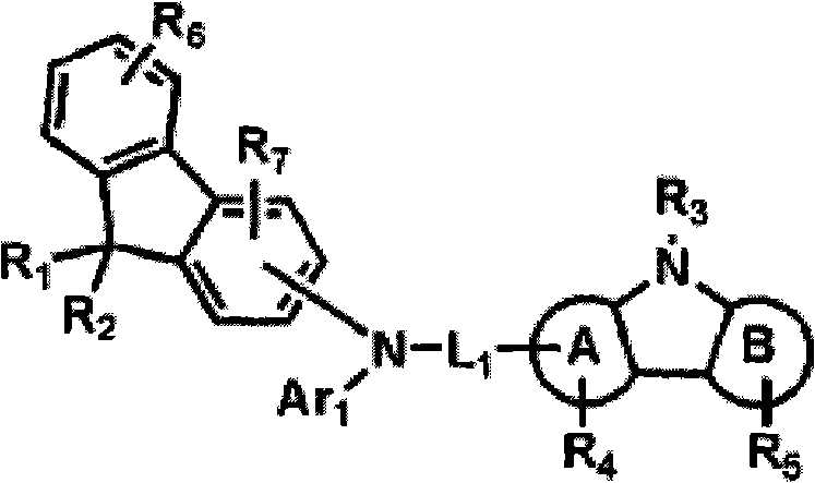
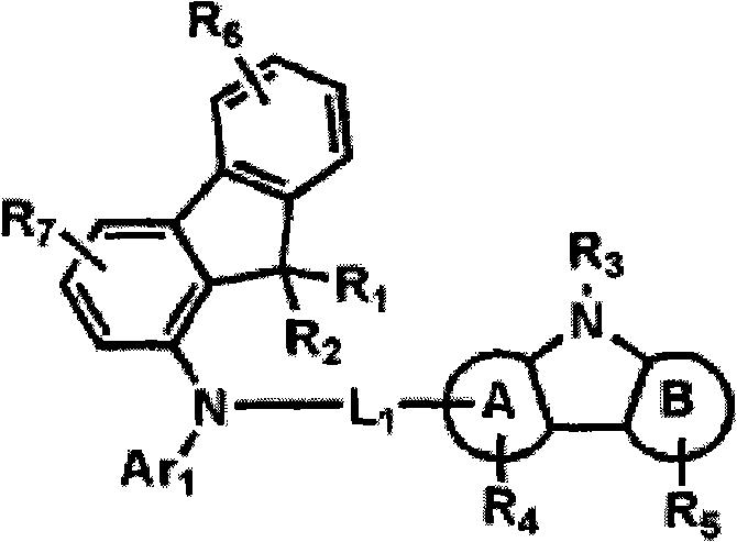
[0065] [Preparation Example 1] Preparation of Compound 4
[0066]
[0067] Preparation of Compound A
[0068] 2-Naphthol (20.0g, 138.8mmol), NaHSO 3 (28.8g, 274.4mmol), distilled water (160mL) and 4-bromophenylhydrazine (31.2mL, 164.4mmol) were heated at 120°C. After 12 hours, distilled water was added and the resulting solid was filtered under reduced pressure. The solid thus obtained was added to aqueous HCl and heated to 100°C. One hour later, after extraction with dichloromethane, the product was washed with distilled water and aqueous NaOH. Column separation gave compound A (9.2 g, 31.0 mmol, 22.4%).
[0069] Preparation of Compound B
[0070] Compound A (9.2g, 31.0mmol), Cu (2.0g, 31.0mmol), 18-crown-6 (0.4g, 1.6mmol), K 2 CO 3 (12.8 g, 93.2 mmol) and 1,2-dichlorobenzene (100 mL) were mixed and stirred under reflux at 180° C. for 12 hours. After cooling to room temperature and distillation under reduced pressure, the product was extracted with dichloromethane ...
Embodiment 1
[0087] [Example 1] Manufacturing OLED devices using the organic electroluminescent compound of the present invention
[0088] OLED devices are fabricated using the organic electroluminescent compounds of the present invention.
[0089] First, the transparent electrode ITO film (15Ω / □) prepared from a glass substrate for OLED (Samsung Corning) was ultrasonically cleaned with trichlorethylene, acetone, ethanol and distilled water in sequence, and stored in isopropanol for future use.
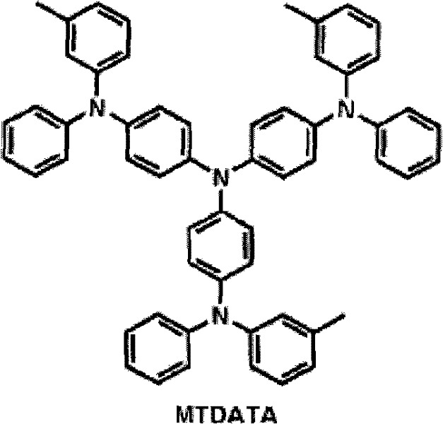
[0090] Next, the ITO substrate was loaded into a substrate holder of a vacuum deposition apparatus. After adding 4,4',4"-three (N, N-(2-naphthyl)-phenylamino) triphenylamine (2-TNATA) in the chamber (cell) of vacuum deposition equipment, the pressure in the chamber dropped to 10 -6 support. Subsequently, 2-TNATA was evaporated by applying a current to the chamber to form a hole injection layer with a thickness of 60 nm on the ITO substrate.
[0091] Thereafter, after compound 1 was added in an...
Embodiment 2
[0106] [Example 2] Preparation of OLED devices using the organic electroluminescent compound of the present invention
[0107] Using the same method as in Example 1, the ITO substrate was mounted on the substrate holder of the vacuum deposition apparatus. After injecting compound 12 into the chamber of vacuum deposition equipment, the pressure in the chamber dropped to 10 -6 support. Subsequently, a current was applied in the chamber to evaporate compound 12 to form a hole injection layer with a thickness of 60 nm on the ITO substrate.
[0108] Next, add N,N'-bis(α-naphthyl)-N,N'-diphenyl-4,4'-diamine (NPB) into another chamber of the vacuum deposition equipment, and apply a current in the chamber NPB was evaporated to form a hole transport layer with a thickness of 20 nm on the hole injection layer.
[0109]
[0110] Remaining process is identical with embodiment 1.
[0111] The fluorescence efficiency of the OLED device that embodiment 2 and comparative example 1 manu...
PUM
| Property | Measurement | Unit |
|---|---|---|
| Thickness | aaaaa | aaaaa |
Abstract
Description
Claims
Application Information