Process for forming optically clear conductive metal or metal alloy thin films and films made therefrom
A conductive metal, optically transparent technology, used in chemical instruments and methods, metal layered products, metal material coating processes, etc., can solve problems such as weakening optical transmittance and increasing resistivity
- Summary
- Abstract
- Description
- Claims
- Application Information
AI Technical Summary
Problems solved by technology
Method used
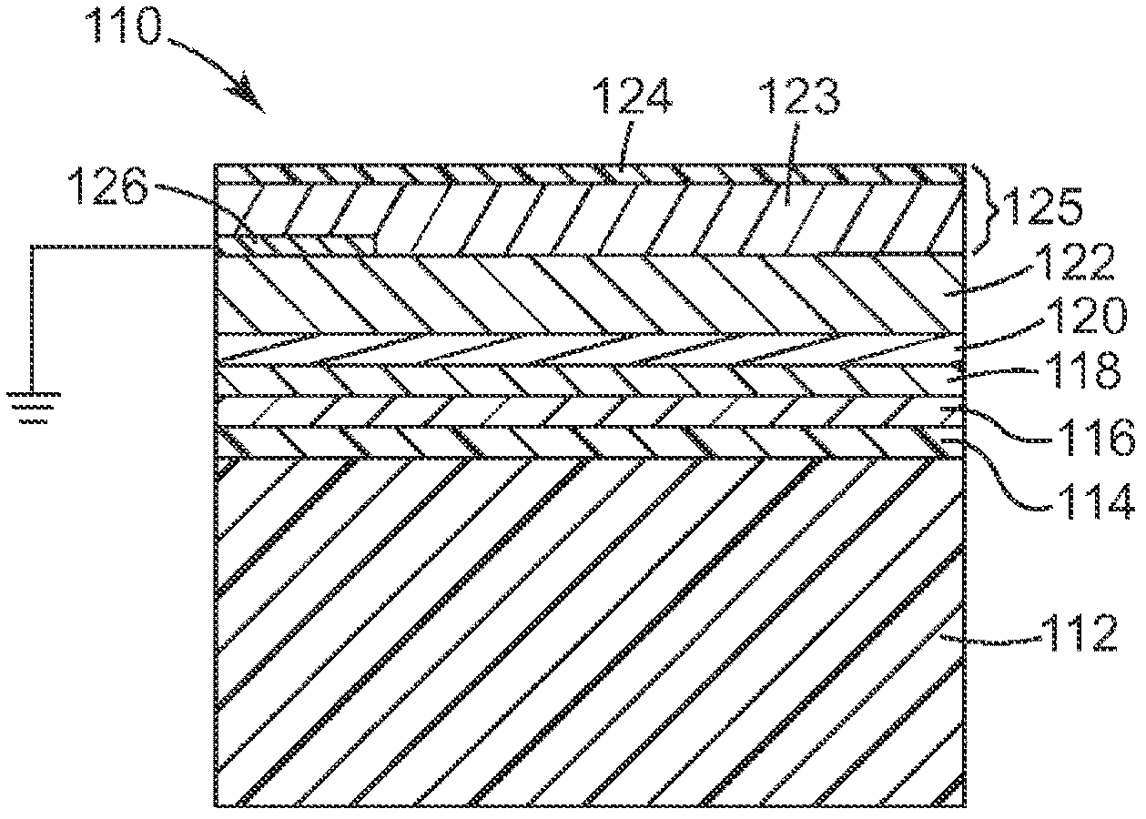
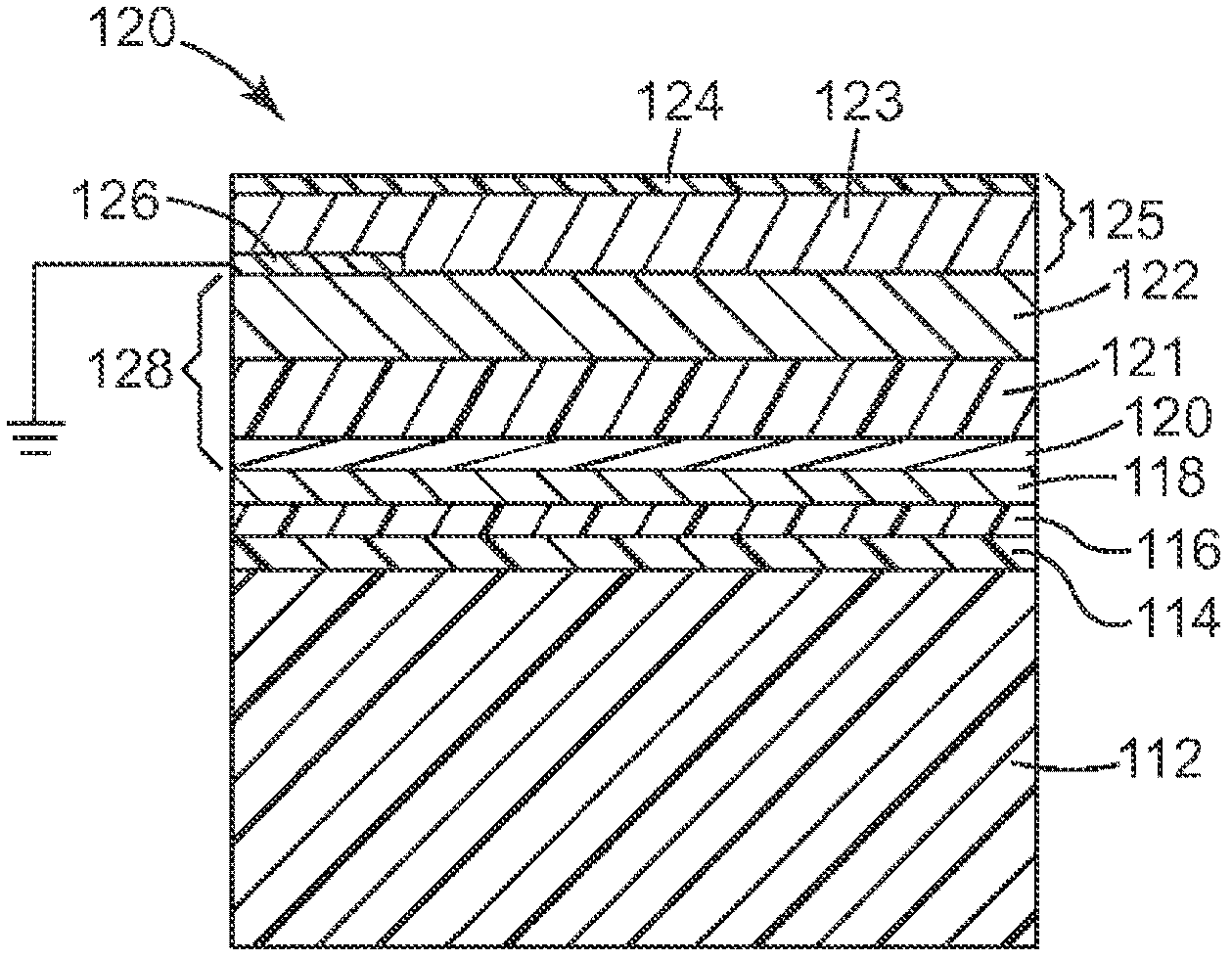
Image

Examples
example
[0058] Table 1
[0059] Materials used for examples
[0060]
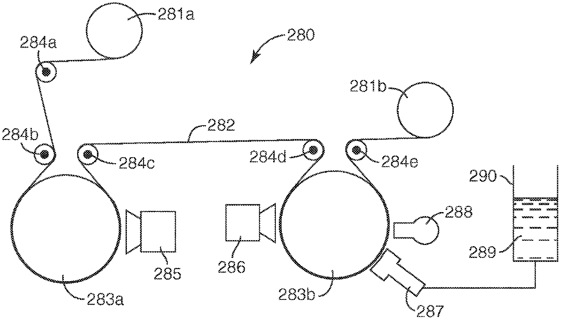
[0061]All examples and comparative examples were prepared using a multi-zone vacuum chamber comprising a roll-to-roll web handling system, which allows for sequential coating and / or treatment processes, including plasma treatment, e-beam treatment, sputter coating and vapor coating. Typically, sequential coating is used to deposit up to three different materials in a single pass through the chamber. Web runs forward unless otherwise indicated. A schematic diagram of the coating system is shown in figure 2 , which is substantially the same as the coating system disclosed, for example, in FIG. 6A of US Patent No. 7,351,479 (Fleming et al.).
[0062] Test Method 1A: Optical Analysis
[0063] Measurements were performed on a BYK Gardner TCS PLUS Spectrophotometer Model 8870 (BYK Gardner Inc., USA) according to ASTM D 1003, E308, CIE 15.2. Percent transmission was measured from 380nm to 720nm using d / 8° g...
example 1
[0087] Example 1 - With SnO 2 layer and the Ag / Au conductive layer of the ZnO seed layer
[0088] The polyester web described in Comparative Example 1A was used. The webs were plasma treated as follows. The pressure of the vacuum chamber is reduced to 5×10 -5 support. Pass nitrogen at a flow rate of 65 sccm through the SnO 2 source is introduced into the vacuum chamber, resulting in a 3.7 x 10 -3 Torr pressure, SnO 2 The source is described in Comparative Example 1A. Plasma treatment was performed at a power of 1000 watts and a line speed of 50 fpm (15 m / min). A first acrylate layer was deposited on the plasma treated web using substantially the same materials and process conditions as described for the preparation of the first acrylate layer of Comparative Example 1A. The polyester web was run in reverse and the first SnO 2 layer with substantially the same materials and process conditions as described in the first sputter-coated SnO 2 layer.
[0089] on the ...
example 2
[0093] Example 2 - With SnO 2 Ag / Au conductive layer for pad layer and ZnO seed layer
[0094] Example 2 was prepared using substantially the same materials, process sequence and process conditions as described in Example 1, with the following modifications. An unprimed polyester web (available under the trade designation "TEIJIN TETORON HB3" from DuPont Teijin Films Ltd.) having a thickness of 2 mils (0.05 mm) and a width of 508 mm was loaded into the drum vacuum chamber. No second SnO deposited 2 layer. The second acrylate layer and the second ZnO / Al 2 o 3 The layers are deposited sequentially adjacent to each other. Additionally, a power level of 2200 watts was used when depositing the first Ag / Au metal alloy layer.
PUM
| Property | Measurement | Unit |
|---|---|---|
| thickness | aaaaa | aaaaa |
| thickness | aaaaa | aaaaa |
| thickness | aaaaa | aaaaa |
Abstract
Description
Claims
Application Information