
Method for measuring thickness of metal film of lithographic mask
A photolithography mask and thickness measurement technology, which is applied in the field of physical measurement, can solve the problem of not using two asymmetric double-sided metal-clad waveguide structures for measurement, and achieves the effects of simple method, convenient operation and noise elimination.
- Summary
- Abstract
- Description
- Claims
- Application Information
AI Technical Summary
Problems solved by technology
Method used
Image

Examples
Embodiment Construction
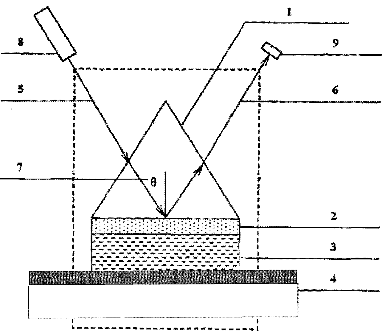
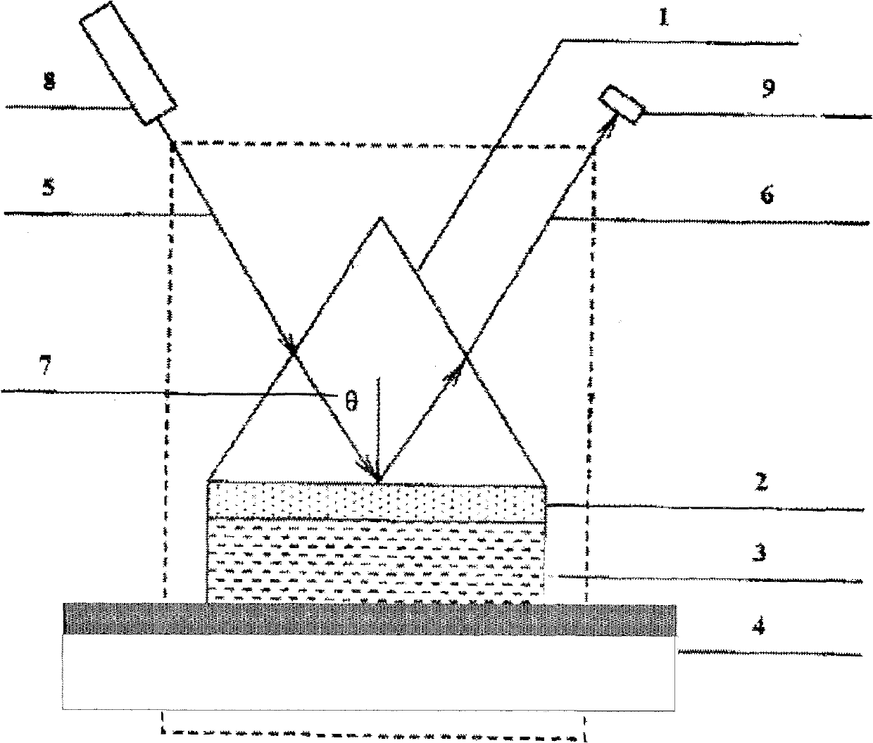
[0025] As shown in the accompanying drawings, the technical solution of the present invention is achieved in this way. The device of the present invention is composed of a coupling device, an upper metal film, an air layer, a lower metal film, and a photolithographic plate metal substrate from top to bottom. The upper metal film, The air layer and the lower metal film are double-sided metal waveguide structures, and the upper and lower metal films are the upper and lower covering layers of the waveguide, and the light is coupled into the waveguide for transmission. The coupling device adopts devices such as high refractive index prism (n>1.5), grating and coupling waveguide, and the shape of the prism can be equilateral, isosceles, or cylindrical according to actual needs. The metal film on the upper layer can generally choose a metal that absorbs less at the working wavelength. The dielectric constant of the metal is related to the working wavelength, and the thickness of the ...
PUM
| Property | Measurement | Unit |
|---|---|---|
| Thickness | aaaaa | aaaaa |
| Thickness | aaaaa | aaaaa |
Abstract
Description
Claims
Application Information