Focusing and leveling detection device and method

A technology of focusing, leveling, and detecting device, which is applied to exposure devices for photoengraving processes, microlithography exposure devices, etc., can solve the problems of low measurement accuracy and small measurement range, and achieves improved measurement accuracy, convenient operation and simple structure. Effect

Active Publication Date: 2009-01-14
SHANGHAI MICRO ELECTRONICS EQUIP (GRP) CO LTD +1
View PDF1 Cites 32 Cited by
  • Summary
  • Abstract
  • Description
  • Claims
  • Application Information

AI Technical Summary

Problems solved by technology

This technology has the characteristics of simple principle, but at the same time, it also has the disadvantages of low measurement accuracy and small measurement range, and the complexity of the mechanical structure is increased due to the use of two optical paths.

Method used


Image

  • Focusing and leveling detection device and method
  • Focusing and leveling detection device and method
  • Focusing and leveling detection device and method

Examples


Embodiment 1

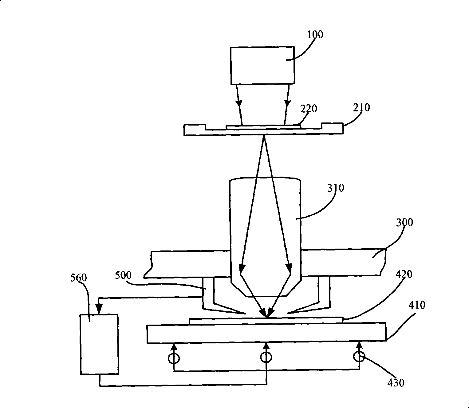
[0042] figure 2 It is a schematic diagram of the plane principle of the optical exposure system. Under the illumination of the illumination system 100 , the light source projects and exposes the image on the mask 220 onto the silicon wafer 420 through the projection objective lens 310 . Mask 220 is supported by mask stage 210 , and silicon wafer 420 is supported by work stage 410 . figure 2Among them, there is a silicon wafer focusing and leveling detection device 500 between the projection objective lens 310 and the silicon wafer 420. This device is rigidly connected with the projection objective lens 310 or the projection objective lens support 300, and is used to perform position information on the surface of the silicon wafer 420. Measurement, the measurement results are sent to the silicon wafer surface position control system 560, after signal processing and calculation of the focusing and leveling amount, the focusing and leveling actuator 430 is driven to adjust the...

Embodiment 2

[0054] This embodiment has the same basic principle structure as that of the aforementioned Embodiment 1, except that the slits in the projection unit use a slit array, and the detection slits use a slit array. The details are as follows:

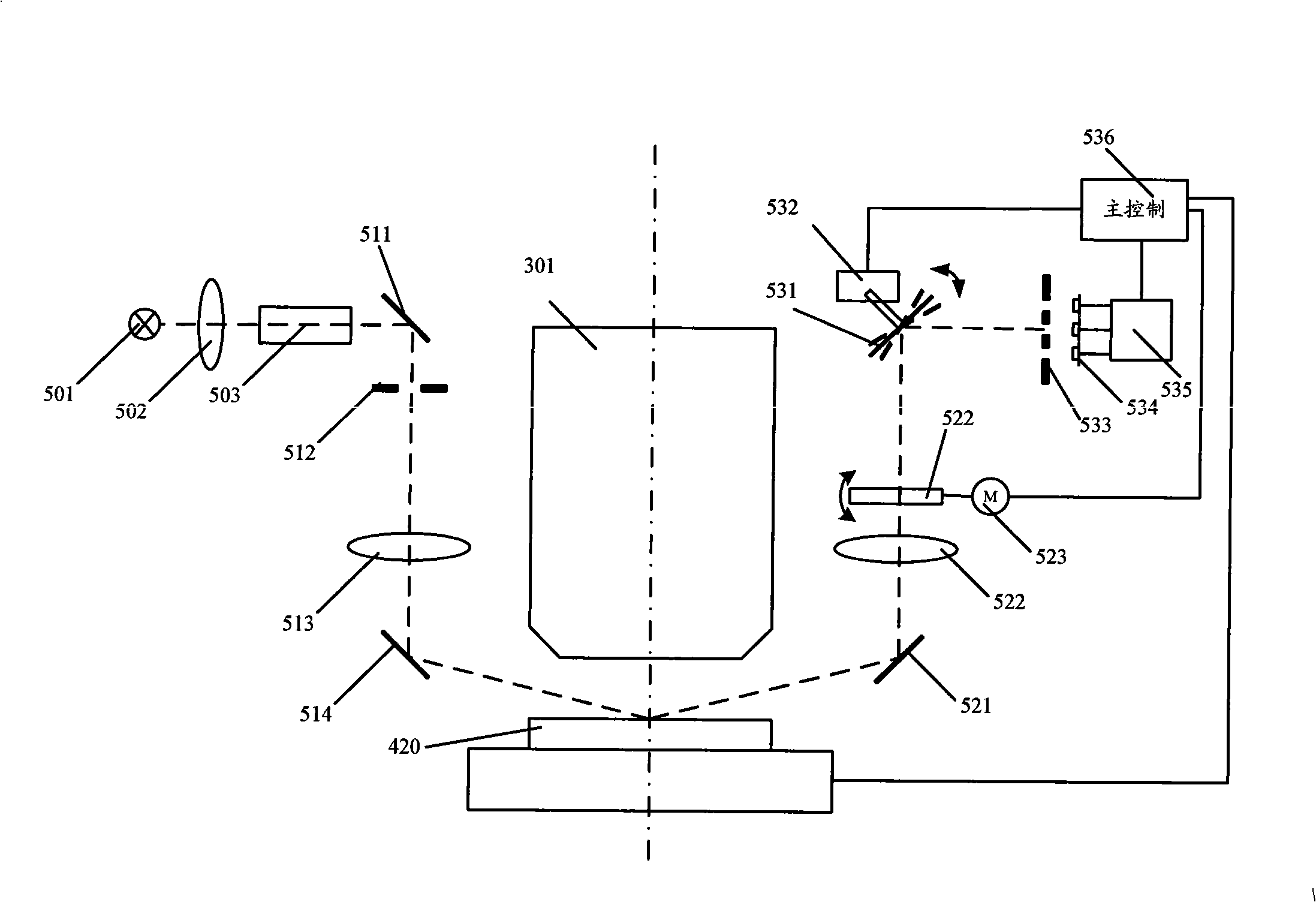
[0055] Figure 12 It is a schematic diagram of the overall structure of this embodiment. The difference from Embodiment 1 is that the slit 512 of the projection unit becomes a slit array of 513; the spot projected by the projection unit on the silicon wafer becomes a spot array 601; Some or all of the light spots have a one-to-many relationship with the detection slit array 537 and the photodetector array 538.

[0056] Figure 13 It is a schematic diagram of signal crosstalk of multiple photodetectors. This embodiment adopts a multi-point arrangement, and if the distance between the light spots is small, signal crosstalk may occur. If the distance between the light spots is small, when the defocus amount of the silicon wafer is large, t...


PUM


Abstract

The invention discloses a focusing-leveling detection apparatus and a corresponding method. A measurement optical-path of the apparatus is respectively arranged on two sides of an optical axis of a projection lens; the apparatus consists of a lighting unit, a projection unit, an imaging unit and a detection unit and is characterized in that one of a plurality of detection slits in a detection slit array corresponding to a light spot is used for precision measurements and the other slits are used for rough measurements; a plurality of detection slits and detectors are adopted to detect the position of one light spot according to the one-to-one corresponding relation between the slits and detectors so as to realize the height and tilt measurements to a silicon plate surface with high accuracy in a wide range; characteristic elements are replaced and a plurality of detection slits are taken from the detection slit array and then are arranged into lines to realize the height and tilt measurements to the silicon plate surface with high accuracy in a wide range in virtue of redundant detection slits. The method is processed sequentially as follows: the processing to signals from detectors; the judgment by the detection slits and the output of measurement results. The invention has the advantages of simple structure and high measurement accuracy.

Description

technical field [0001] The invention relates to a device and method for coordinating with a projection photolithography machine to perform focus adjustment and leveling measurement on a silicon wafer used for manufacturing microelectronic products. Background technique [0002] In a projection lithography device, a silicon wafer focusing and leveling detection device is usually used to measure the height and inclination of a specific area on the silicon wafer surface. The measurement device requires high precision, and the silicon wafer cannot be damaged during operation. Therefore, the silicon wafer focusing and leveling measurement must be non-contact measurement. There are three commonly used non-contact focusing and leveling measurement methods: optical measurement method, capacitance measurement method, and air pressure measurement method. [0003] In today's scanning projection lithography apparatuses, optical measurement methods are often used to achieve focus and le...

Claims


Application Information

Patent Timeline
Patent Type & Authority Applications(China)
IPC IPC(8): G03F7/20
Inventor 廖飞红李志丹李小平程吉水李志科
Owner SHANGHAI MICRO ELECTRONICS EQUIP (GRP) CO LTD
Why Eureka
Try Eureka