
All-digital clock data recovery device and transceiver implemented thereof

A clock data recovery and clock technology, applied in the direction of digital transmission system, synchronous receiver, automatic power control, etc., can solve the problem that it is difficult to form a charge excitation circuit

Inactive Publication Date: 2012-05-30
GLOBAL NETWORKS & SYST +1
View PDF4 Cites 9 Cited by
  • Summary
  • Abstract
  • Description
  • Claims
  • Application Information

AI Technical Summary

Problems solved by technology

[0014] Therefore, it will be difficult to form an analog circuit mode charge excitation circuit in an integrated circuit project with a power supply voltage below 1.0V.

Method used


Image

  • All-digital clock data recovery device and transceiver implemented thereof
  • All-digital clock data recovery device and transceiver implemented thereof
  • All-digital clock data recovery device and transceiver implemented thereof

Examples


Embodiment Construction

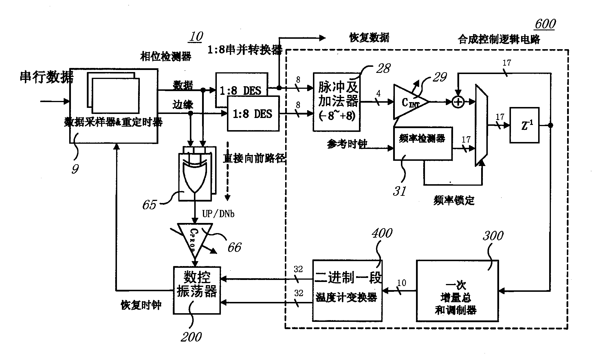
[0032] As a representative embodiment of the present invention, the PMOS transistor array (array) is composed of a variable resistance switching matrix, and the current of the PMOS transistor will be controlled according to the input signal of the logic gate, and will function as a variable resistance. At this time, the present invention proposes a method of inserting vertical resistors between rows of the switching matrix in order to equalize the low-bit frequency tuning step and the high-bit frequency tuning step. Obviously the vertical resistors consist of PMOS transistors and the logic gates are grounded.

[0033] In addition, in order to eliminate the jitter caused by the quantization error when the digitally controlled oscillator (DCO) is compared with the analog mode voltage controlled oscillator (VCO), in the present invention, the jitter ( Dithering) algorithm, for example, in order to ensure 17-bit resolution, 10-bit MSB and 7-bit LSB are dithered to prevent errors e...


PUM


Abstract

The present invention relates to a clock data recovery apparatus having all circuits thereof digital-circuitized through a digital filter and a digitally controlled oscillator (DCO). A DCO according to the present invention has a chain of plural inverters, and a variable resistance switch matrix is configured between the inverters and a voltage source for supplying a source current to each of the inverters to tune the oscillation frequency through variation of a supply voltage. Here, the variable resistance switch matrix is implemented by using a PMOS transistor array, and meanwhile a vertical resistance is further inserted between columns of the switch matrix to equalize between the frequency tuning step at a lower level and the frequency tuning step at a high level. Also, to resolve the occurrence of jitter problems, a primary sigma delta modulator is used for implementing a dithering circuit and a segment thermometer scheme is applied to tune a DCO with a smaller number of routing lines.

Description

technical field [0001] The present invention relates to a clock data recovery (clock data recovery; CDR) and its related transceiver (transceiver), especially a clock data recovery device, which recovers a clock signal and data from a data bit stream (bit stream) input in a serial data communication mode There are no analog circuits in all the circuits, only digital circuits. Background technique [0002] Recently, gigabit per second (GB / s) high-speed serial interface (serial link) communication methods have become popular, and serial interface transceivers are installed in a single chip. These serial interface chip-to-chip (chip-to-chip) chip) communication, in order to prevent the receiving side from transmitting a clock signal separately, only data is transmitted through the communication channel. Therefore, clock data recovery (CDR) for retrieving clock information and data information from the serial data bits is required in order to process gigabits per second serial ...

Claims


Application Information

Patent Timeline
Patent Type & Authority Applications(China)
IPC IPC(8): H03L7/08H04L7/00
CPCH03L7/0995H04L7/0079H03L7/0807H04L7/033H04L7/0331H03L7/093H03L7/099H04B1/06
Inventor 郑德均吴道焕
Owner GLOBAL NETWORKS & SYST
Learn More